The following content is an automatically extracted verbatim text
from the original manufacturer datasheet and is provided for reference purposes only.
View original datasheet text
HM4611Q
N And P-Channel Enhancement Mode MOSFET
Description
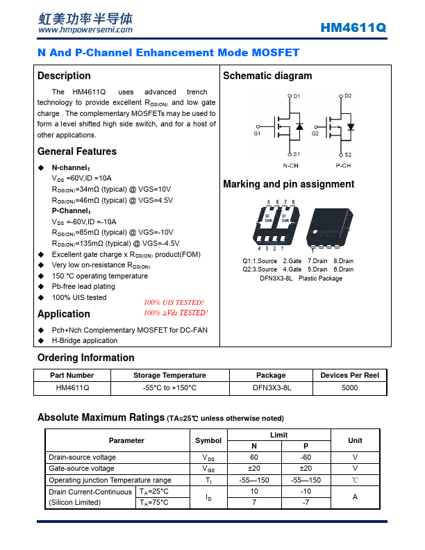
Schematic diagram
The HM4611Q uses advanced trench technology to provide excellent RDS(ON) and low gate charge . The complementary MOSFETs may be used to form a level shifted high side switch, and for a host of other applications.
General Features
N-channel:
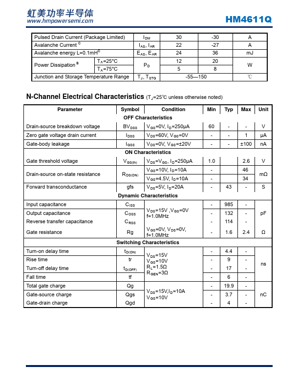
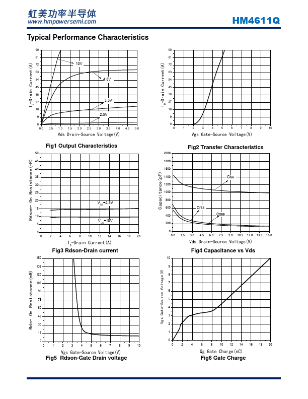
VDS =60V,ID =10A RDS(ON)=34mΩ (typical) @ VGS=10V RDS(ON)=46mΩ (typical) @ VGS=4.5V P-Channel:
VDS =-60V,ID =-10A RDS(ON)=85mΩ (typical) @ VGS=-10V RDS(ON)=135mΩ (typical) @ VGS=-4.5V Excellent gate charge x RDS(ON) product(FOM) Very low on-resistance RDS(ON) 150 °C operating temperature
Pb-free lead plating
100% UIS tested
100% UIS TESTED!
Application
100% ∆Vds TESTED!
Marking and pin assignment
Q1:1.Source 2.Gate 7.Drain 8.Drain Q2:3.Source 4.
 HM4611Q Datasheet