The following content is an automatically extracted verbatim text
from the original manufacturer datasheet and is provided for reference purposes only.
View original datasheet text
2SJ517
Silicon P Channel MOS FET High Speed Power Switching
ADE-208-575B (Z) 3rd. Edition Jun 1998 Features
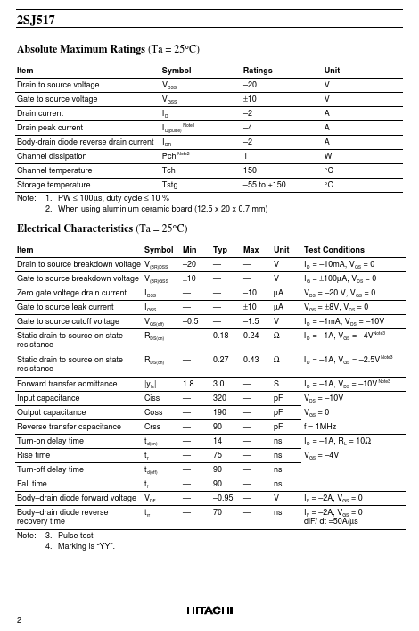
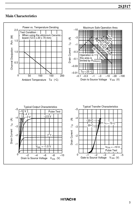
• Low on-resistance R DS(on) = 0.18 Ω typ. (at V GS =–4V, ID =–1A) • Low drive current • High speed switching • 2.5V gate drive devices.
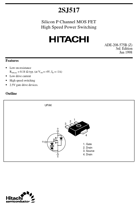
Outline
UPAK
3
D
2
1
4
G
S
1. Gate 2. Drain 3. Source 4. Drain
2SJ517
Absolute Maximum Ratings (Ta = 25°C)
Item Drain to source voltage Gate to source voltage Drain current Drain peak current Body-drain diode reverse drain current Channel dissipation Channel temperature Storage temperature Note: Symbol VDSS VGSS ID I D(pulse) I DR Pch Tch Tstg
Note2 Note1
Ratings –20 ±10 –2 –4 –2 1 150 –55 to +150
Unit V V A A A W °C °C
1. PW ≤ 100 µs, duty cycle ≤ 10 % 2. When using aluminium ceramic board (12.5 x 20 x 0.