2SJ574 Overview
Key Features
- Low on-resistance R DS = 1.1 Ω typ. (VGS = -10 V , I D = -150 mA) R DS = 2.2 Ω typ. (VGS = -4 V , I D = -150 mA)
- 4 V gate drive device
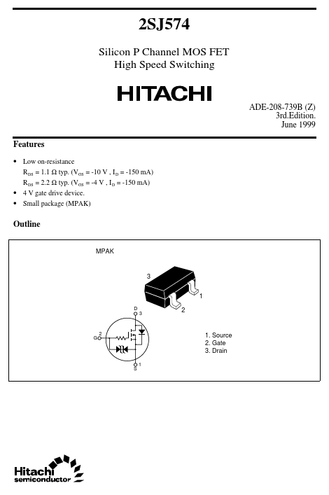
- Small package (MPAK) Outline MPAK 3 1 D 3 2 2 G
- Drain S 1 2SJ574
| Part | 2SJ574 |
|---|---|
| Description | Silicon P-Channel MOSFET |
| Category | MOSFET |
| Manufacturer | Hitachi Semiconductor |
| Size | 39.95 KB |
| Part Number | Manufacturer | Description |
|---|---|---|
| 2SJ574 | Renesas | P-Channel MOSFET |
| 2SJ578 | SANYO | Ultrahigh-Speed Switching Applications |
| 2SJ579 | SANYO | Ultrahigh-Speed Switching Applications |