Datasheet Summary
Silicon P Channel MOS FET High Speed Switching
ADE-208-802 (Z) 1st.Edition. June 1999 Features
- Low on-resistance R DS =2.8 Ω typ. (V GS = -10 V , I D = -50 mA) R DS =5.7 Ω typ. (V GS = -4 V , I D = -50 mA)
- 4 V gate drive device.
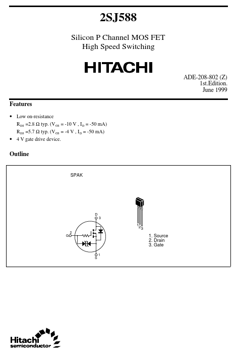
Outline
SPAK
D 3
12 3
2 G
1. Source 2. Drain 3. Gate
S...