HD74HCT533
HD74HCT533 is Octal D-type Transparent Latches(with inverted 3-state outputs) manufactured by Hitachi Semiconductor.
HD74HCT373/HD74HCT533
Octal D-type Transparent Latches (with 3-state outputs)/ Octal D-type Transparent Latches (with inverted 3-state outputs)
Description
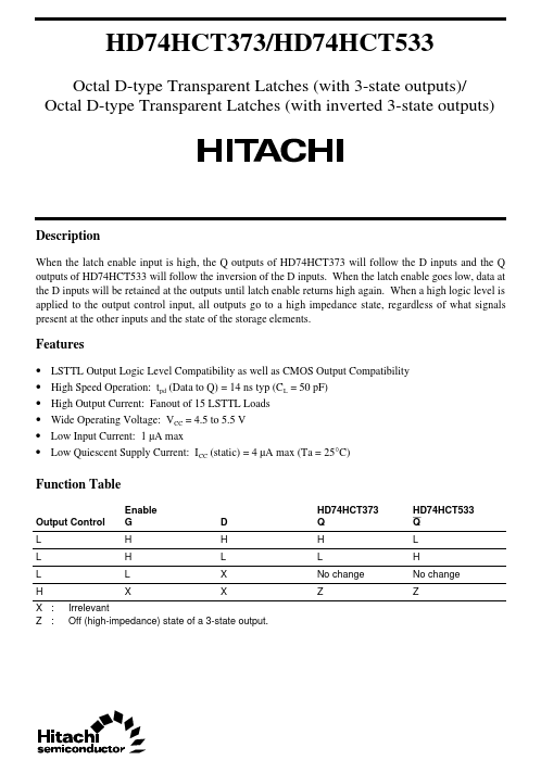
When the latch enable input is high, the Q outputs of HD74HCT373 will follow the D inputs and the Q outputs of HD74HCT533 will follow the inversion of the D inputs. When the latch enable goes low, data at the D inputs will be retained at the outputs until latch enable returns high again. When a high logic level is applied to the output control input, all outputs go to a high impedance state, regardless of what signals present at the other inputs and the state of the storage elements.
Features
- -
- -
- - LSTTL Output Logic Level patibility as well as CMOS Output patibility High Speed Operation: tpd (Data to Q) = 14 ns typ (CL = 50 p F) High Output Current: Fanout of 15 LSTTL Loads Wide Operating Voltage: VCC = 4.5 to 5.5 V Low Input Current: 1 µA max Low Quiescent Supply Current: ICC (static) = 4 µA max (Ta = 25°C)
Function Table
Output Control L L L H X : Z : Enable G H H L X D H L X X HD74HCT373 Q H L No change Z HD74HCT533 Q L H No change Z
Irrelevant Off (high-impedance) state of a 3-state output.
HD74HCT373/HD74HCT533
Pin Arrangement
HD74HCT373
Output Control 1 1Q 1D 2D 2Q 3Q 3D 4D 4Q 2 3 4 5 6 7 8 9
20 VCC 19 8Q 18 8D 17 7D 16 7Q 15 6Q 14 6D 13 5D 12 5Q 11 Enable G (Top view)
GND 10
Output Control 1 1Q 1D 2D 2Q 3Q 3D 4D 4Q 2 3 4 5 6 7 8 9
20 VCC 19 8Q 18 8D 17 7D 16 7Q 15 6Q 14 6D 13 5D 12 5Q 11 Enable G (Top view)
GND 10
HD74HCT373/HD74HCT533
Block Diagram
HD74HCT373
1D D GQ Enable G 2D D GQ 3D D GQ 4D D GQ 5D D GQ 6D D GQ 7D D GQ 8D D GQ
Output Control 1Q 2Q 3Q 4Q 5Q 6Q 7Q 8Q
1D D GQ Enable G 2D D GQ 3D D GQ 4D D GQ 5D D GQ 6D D GQ 7D D GQ 8D D GQ
Output Control 1Q 2Q 3Q 4Q 5Q 6Q 7Q 8Q
HD74HCT373/HD74HCT533...