HD74HCT564
HD74HCT564 is Octal D-type Flip-Flops (with 3-state outputs) manufactured by Hitachi Semiconductor.
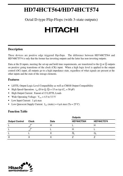
HD74HCT564/HD74HCT574
Octal D-type Flip-Flops (with 3-state outputs)
Description
These devices are positive edge triggered flip-flops. The difference between HD74HCT564 and HD74HCT574 is only that the former has inverting outputs and the latter has non-inverting outputs. Data at the D inputs, meeting the set-up and hold time requirements, are transferred to the Q or Q outputs on positive going transitions of the clock (CK) input. When a high logic level is applied to the output control (OC) input, all outputs go to a high impedance state, regardless of what signals are present at the other inputs and the state of the storage elements.
Features
- -
- -
- - LSTTL Output Logic Level patibility as well as CMOS Output patibility High Speed Operation: tpd (D to Q, Q) = 15 ns typ (CL = 50 p F) High Output Current: Fanout of 15 LSTTL Loads Wide Operating Voltage: VCC = 4.5 to 5.5 V Low Input Current: 1 µA max Low Quiescent Supply Current: ICC (static) = 4 µA max (Ta = 25°C)
Function Table
Outputs Output Control L L L H L X Clock Data H L X X HD74HCT564 L H Q0 Z HD74HCT574 H L Q0 Z
HD74HCT564/HD74HCT574
Pin Arrangement
Output Control 1 1D 2 2D 3 3D 4 4D 5 5D 6 6D 7 7D 8 8D 9 GND 10
OE D Q OE D Q OE D Q OE D Q OE D Q OE D Q OE D Q OE D Q
20 VCC 19 1Q 18 2Q 17 3Q 16 4Q 15 5Q 14 6Q 13 7Q 12 8Q 11 Clock
(Top view)
HD74HCT564/HD74HCT574
HD74HCT574
Output Control 1 1D 2 2D 3 3D 4 4D 5 5D 6 6D 7 7D 8 8D 9 GND 10
OE D Q OE D Q OE D Q OE D Q OE D Q OE D Q OE D Q OE D Q
20 VCC 19 1Q 18 2Q 17 3Q 16 4Q 15 5Q 14 6Q 13 7Q 12 8Q 11 Clock
(Top view)
HD74HCT564/HD74HCT574
Block Diagram
1D 2D 3D
D C Q C D C Q C D C Q C D C Q C D C Q C D C Q C D C Q C D C Q C
1Q 2Q 3Q 4Q 5Q 6Q 7Q 8Q
4D 5D 6D 7D 8D CLK OC
HD74HCT564/HD74HCT574
HD74HCT574...