3SK290
3SK290 is Silicon N-Channel Dual Gate MOS FET manufactured by Hitachi Semiconductor.
Features
- Low noise figure. NF = 2.3 d B Typ. at f = 900 MHz
- High gain. PG = 19.3 d B Typ. at f = 900 MHz
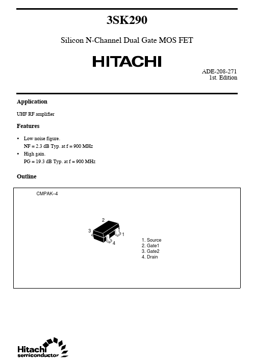
Outline
CMPAK- 4
2 3 4 1 1. Source 2. Gate1 3. Gate2 4. Drain
Absolute Maximum Ratings (Ta = 25¡C)
Item Drain to source voltage Gate 1 to source voltage Gate 2 to source voltage Drain current Channel power dissipation Channel temperature Storage temperature Symbol VDS VG1S VG2S ID Pch Tch Tstg Ratings 12 ±8 ±8 25 100 125
- 55 to +125 Unit V V V m A m W °C °C
Attention: This device is very sensitive to electro static discharge. It is remended to adopt appropriate cautions when handling this transistor.
Electrical Characteristics (Ta = 25¡C)
Item Drain to source breakdown voltage Gate 1 to source breakdown voltage Gate 2 to source breakdown voltage Gate 1 cutoff current Gate 2 cutoff current Drain current Symbol V(BR)DSX V(BR)G1SS V(BR)G2SS I G1SS I G2SS I DS(on) Min 12 ±8 ±8
- - 0.5
- 0.6 0 16 1.2 0.7
- 17
- Typ
- -
- -
- -
- - 22 1.8 1.2 0.02 19.3 2.3 Max
- -
- ±100 ±100 10 +0.5 +1.0
- 2.2 1.4 0.03
- 2.8 Unit V V V n A n A m A V V m S p F p F p F d B d B VDS = 4 V, VG2S = 3 V, I D = 10 m A, f = 900 MHz Test conditions I D = 200 m A, VG1S =
- 3 V, VG2S =
- 3 V I G1 = ±10 m A, VG2S = VDS = 0 I G2 = ±10 m A, VG1S = VDS = 0 VG1S = ±6 V, V G2S = VDS = 0 VG2S = ±6 V, V G1S = VDS = 0 VDS = 6 V, VG1S = 0.5 V, VG2S = 3 V VDS = 10 V, VG2S = 3 V, I D = 100 m A VDS = 10 V, VG1S = 3 V, I D = 100 m A VDS = 6 V, VG2S = 3 V, I D = 10 m A, f = 1 k Hz VDS = 6 V, VG2S = 3V, I D = 10 m A, f = 1 MHz
Gate 1 to source cutoff voltage VG1S(off) Gate 2 to source cutoff voltage VG2S(off) Forward transfer admittance Input capacitance Output capacitance Reverse transfer capacitance Power gain Noise figure Note: Marking is “ZJ- ”. |yfs| Ciss Coss Crss PG NF
Maximum Channel Power Dissipation Curve Pch (m W) 200 Typical Output Characteristics VG2S = 3 V 1.2 V 150 I D (m A) 16 1.0 V
Channel Power Dissipation
0.8 V
Drain Current
0.6 V 0.4 V VG1S = 0.2V
50...