HAF2001
HAF2001 is Silicon N Channel MOS FET Series Power Switching manufactured by Hitachi Semiconductor.
Features
This FET has the over temperature shut- down capability sensing to the junction temperature. This FET has the built- in over temperature shut- down circuit in the gate area. And this circuit operation to shut- down the gate voltage in case of high junction temperature like applying over power consumption, over current etc.
- Logic level operation (4 to 6 V Gate drive)
- High endurance capability against to the short circuit
- Built- in the over temperature shut- down circuit
- Latch type shut- down operation (Need 0 voltage recovery)
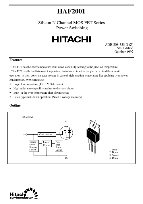
Outline
TO- 220AB
D 4
Gate resistor
Tempe- rature Sencing Circuit
Latch Circuit
Gate Shut- down Circuit
1 2 S 3
1. Gate 2. Drain 3. Source 4. Drain
Absolute Maximum Ratings (Ta = 25°C)
Item Drain to source voltage Gate to source voltage Gate to source voltage Drain current Drain peak current Body-drain diode reverse drain current Channel dissipation Channel temperature Storage temperature Note: 1. PW ≤ 10 µs, duty cycle ≤ 1 % 2. Value at Ta = 25°C Symbol VDSS VGSS VGSS ID I D(pulse) I DR Pch Tch Tstg
Note2 Note1
Ratings 60 16
- 2.8 20 40 20 50 150
- 55 to +150
Unit V V V A A A W °C °C
Typical Operation Characteristics
Item Input voltage Symbol VIH VIL Input current (Gate non shut down) I IH1 I IH2 I IL Input current (Gate shut down) Shut down temperature Gate operation voltage I IH(sd)1 I IH(sd)2 Tsd VOP Min 3.5
- -
- -
- -
- 3.5 Typ
- -
- -
- 0.8 0.35 175
- Max
- 1.2 100 50 1
- -
- 13 Unit V V µA µA µA m A m A °C V Vi = 8V, VDS = 0 Vi = 3.5V, VDS = 0 Vi = 1.2V, VDS = 0 Vi = 8V, VDS = 0 Vi = 3.5V, VDS = 0 Channel temperature Test Conditions
Electrical Characteristics (Ta = 25°C)
Item Drain current Drain current Drain to source breakdown voltage Gate to source breakdown voltage Gate to source breakdown voltage Gate to source leak current Symbol I D1 I D2 V(BR)DSS V(BR)GSS V(BR)GSS I GSS1 I GSS2 I GSS3 I GSS4 Input current (shut down) I GS(op)1 I GS(op)2 Zero gate voltege drain current I DSS Min 10
- 60 16
-...