HD74HCT1G04
HD74HCT1G04 is High speed CMOS inverter using silicon gate CMOS process manufactured by Hitachi Semiconductor.
Description
The HD74HCT1G04 is high speed CMOS inverter using silicon gate CMOS process. With CMOS low power dissipation, it provides high speed equivalent to LS- TTL series. The internal circuit of three stages construction with buffer provides wide noise margin and stable output.
Features
- The basic gate function is lined up as hitachi uni logic series.
- Supplied on emboss taping for high speed automatic mounting.
- TTL patible input level. Supply voltage range : 4.5 to 5.5 V Operating temperature range :
- 40 to +85°C
- |IOH| = IOL = 2 m A (min)
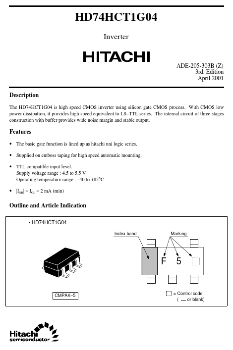
Outline and Article Indication
- HD74HCT1G04
Index band Marking
CMPAK- 5
= Control code ( or blank)
Function Table
Input A H L H : High level L : Low level Output Y L H
Pin Arrangement
IN Y
OUT Y
(Top view)
Absolute Maximum Ratings
Item Supply voltage range Input voltage range
- 1
- 1, 2
Symbol VCC VI VO I IK I OK IO
Ratings
- 0.5 to 7.0
- 0.5 to VCC + 0.5
- 0.5 to VCC + 0.5 ±20 ±20 ±25 ±25 200
- 65 to 150
Unit V V V m A m A m A m A m W °C
Test Conditions
Output voltage range Input clamp current Output clamp current
Output : H or L VI < 0 or VI > VCC VO < 0 or VO >VCC VO = 0 to VCC
Continuous output current
Continuous current through I CC or IGND VCC or GND Maximum power dissipation PT at Ta = 25°C (in still air)
- 3 Storage temperature Notes: Tstg
The absolute maximum ratings are values which must not individually be exceeded, and furthermore, no two of which may be realized at the same time. 1. The input and output voltage ratings may be exceeded if the input and output clamp-current ratings are observed. 2. This value is limited to 5.5 V maximum. 3. The maximum package power dissipation was caluculated using a junction temperature of...