K1164
K1164 is 2SK1164 manufactured by Hitachi Semiconductor.
Features
- -
- -
- Low on-resistance High speed switching Low drive current No secondary breakdown Suitable for switching regulator and DC-DC converter
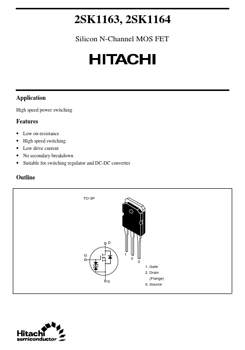
Outline
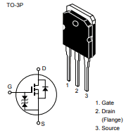
TO-3P
D G 1 2 3 1. Gate 2. Drain (Flange) 3. Source
2SK1163, 2SK1164
Absolute Maximum Ratings (Ta = 25°C)
Item Drain to source voltage 2SK1163 2SK1164 Gate to source voltage Drain current Drain peak current Body to drain diode reverse drain current Channel dissipation Channel temperature Storage temperature Notes: 1. PW ≤ 10 µs, duty cycle ≤ 1% 2. Value at TC = 25°C VGSS ID I D(pulse)- I DR Pch- Tch Tstg
2 1
Symbol VDSS
Ratings 450 500 ±30 11 40 11 100 150
- 55 to +150
Unit V
V A A A W °C °C
2SK1163, 2SK1164
Electrical Characteristics (Ta = 25°C)
Item Drain to source breakdown voltage Symbol Min 2SK1163 V(BR)DSS 2SK1164 V(BR)GSS I GSS 450 500 ±30
- -
- -
- - ±10 250 V µA µA I G = ±100 µA, VDS = 0 VGS = ±25 V, VDS = 0 VDS = 360 V, VGS = 0 VDS = 400 V, VGS = 0 VGS(off) 2.0
- - |yfs| Ciss Coss Crss t d(on) tr t d(off) tf VDF t rr 5.0
- -
- -
- -
- -
- - 0.55 0.60 8.0 1150 340 55 17 60 95 50 1.0 400 3.0 0.7 0.8
- -
- -
- -
- -
- - S p F p F p F ns ns ns ns V ns I F = 11 A, VGS = 0 I F = 11 A, VGS = 0, di F/dt = 100 A/µs I D = 5 A, VGS = 10 V, RL = 6 Ω I D = 5 A, VDS = 10 V
- 1 VDS = 10 V, VGS = 0, f = 1 MHz V Ω I D = 1 m A, VDS = 10 V I D = 5 A, VGS = 10 V
- 1 Typ
- Max
- Unit V Test conditions I D = 10 m A, VGS = 0
Gate to source breakdown voltage Gate to source leak current Zero gate voltage drain...
Representative K1164 image (package may vary by manufacturer)