K1329
K1329 is 2SK1329 manufactured by Hitachi Semiconductor.
Features
- -
- -
- Low on-resistance High speed switching Low drive current No secondary breakdown Suitable for switching regulator and DC-DC converter
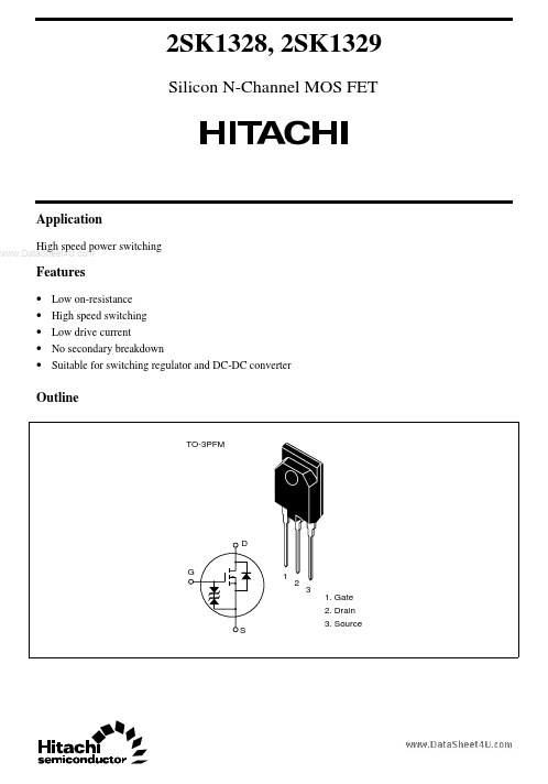
Outline
TO-3PFM
1. Gate 2. Drain 3. Source
2SK1328, 2SK1329
Absolute Maximum Ratings (Ta = 25°C)
Item Drain to source voltage 2SK1328 2SK1329 Gate to source voltage Drain current Drain peak current Body to drain diode reverse drain current Channel dissipation Channel temperature Storage temperature
..
Symbol VDSS
Ratings 450 500 ±30 12
Unit V
VGSS ID I D(pulse)- I DR Pch- Tch Tstg
2 1
V A A A W °C °C
48 12 60 150
- 55 to +150
Notes: 1. PW ≤ 10 µs, duty cycle ≤ 1% 2. Value at TC = 25°C
2SK1328, 2SK1329
Electrical Characteristics (Ta = 25°C)
Item Drain to source breakdown voltage Symbol Min 2SK1328 V(BR)DSS 2SK1329 V(BR)GSS I GSS 450 500 ±30
- -
- -
- - ±10 250 V µA µA I G = ±100 µA, VDS = 0 VGS = ±25 V, VDS = 0 VDS = 360 V, VGS = 0 VDS = 400 V, VGS = 0 VGS(off) 2.0
- - |yfs| Ciss Coss Crss t d(on) tr t d(off) tf VDF t rr 6.0
- -
- -
- -
- -
- - 0.40 0.45 10 1450 410 55 20 70 120 60 1.0 450 3.0 0.55 0.60
- -
- -
- -
- -
- - S p F p F p F ns ns ns ns V ns I F = 12 A, VGS = 0 I F = 12 A, VGS = 0, di F/dt = 100 A/µs I D = 6 A, VGS = 10 V, RL = 5 Ω I D = 6 A, VDS = 10 V
- 1 VDS = 10 V, VGS = 0, f = 1 MHz V Ω I D = 1 m A, VDS = 10 V I D = 6 A, VGS = 10...