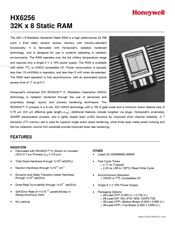
HX6256
HX6256 is 32K x 8 Static RAM manufactured by Honeywell.
feature size of 0.75 µm (0.6 µm effective gate length- Leff). Additional features include tungsten via plugs, Honeywell’s proprietary SHARP planarization process, and a lightly doped drain (LDD) structure for improved short channel reliability. A 7 transistor (7T) memory cell is used for superior single event upset hardening, while three layer metal power bussing and the low collection volume SOI substrate provide improved dose rate hardening.
FEATURES
RADIATION
- Fabricated with RICMOS™ IV Silicon on Insulator (SOI) 0.7 µm Process (Leff = 0.6 µm)
- -
- -
- - Total Dose Hardness through 1x10⁶ rad(Si O2) Neutron Hardness through 1x1014 cm-2 Dynamic and Static Transient Upset Hardness through 1x10⁹ rad(Si)/s Dose Rate Survivability through 1x10¹¹ rad(Si)/s Soft Error Rate of <1x10⁻¹⁰ upsets/bit-day in Geosynchronous Orbit No Latchup
- -
- OTHER
- Listed On SMD#5962- 95845
- Fast Cycle Times o ≤ 17 ns (Typical) o ≤ 25 ns (-55 to 125°C) Read Write Cycle Asynchronous Operation o CMOS or TTL patible I/O Single 5 V ± 10% Power Supply Packaging Options o 28-Lead CFP (0.500 in. x 0.720 in.) o 28-Lead DIP, MIL-STD-1835, CDIP2-T28 o 36-Lead CFP- Bottom Braze (0.630 x 0.650 in.) o 36-Lead CFP- Top Braze (0.630 x 0.650 in.)
FUNCTIONAL DIAGRAM
..
SIGNAL DEFINITIONS
A: 0-14 Address input pins which select a particular eight-bit word within the memory array.
DQ: 0-7 Bidirectional data pins which serve as data outputs during a read operation and as data inputs during a write operation. NCS Negative chip select, when at a low level allows normal read or write operation. When at a high level NCS forces the SRAM to a precharge condition, holds the data output drivers in a high impedance state and disables all input buffers except CE. If this signal is not used it must be connected to VSS. Negative write enable, when at a low level activates a write operation and holds the data output drivers in a high impedance state. When at a high level NWE allows normal...