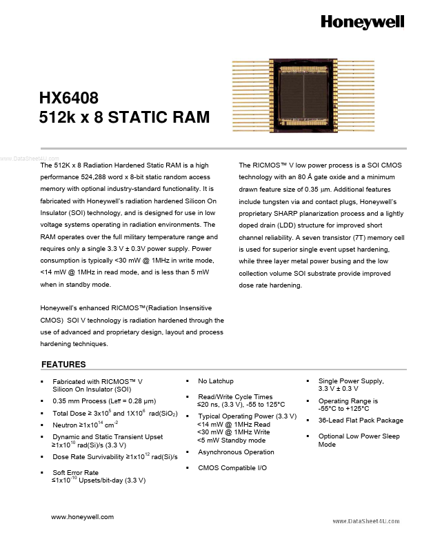
HX6408
HX6408 is 512k x 8 STATIC RAM manufactured by Honeywell.
feature size of 0.35 µm. Additional features include tungsten via and contact plugs, Honeywell’s proprietary SHARP planarization process and a lightly doped drain (LDD) structure for improved short channel reliability. A seven transistor (7T) memory cell is used for superior single event upset hardening, while three layer metal power busing and the low collection volume SOI substrate provide improved dose rate hardening.
FEATURES
- -
- -
- -
- Fabricated with RICMOS™ V Silicon On Insulator (SOI) 0.35 mm Process (Leff = 0.28 µm) Total Dose ≥ 3x10 and 1X10 rad(Si O2) Neutron ≥1x10 cm
14 -2 5 6
- -
- No Latchup Read/Write Cycle Times ≤20 ns, (3.3 V), -55 to 125°C Typical Operating Power (3.3 V) <14 m W @ 1MHz Read <30 m W @ 1MHz Write <5 m W Standby mode Asynchronous Operation CMOS patible I/O
- -
- -
Single Power Supply, 3.3 V ± 0.3 V Operating Range is -55°C to +125°C 36-Lead Flat Pack Package Optional Low Power Sleep Mode
Dynamic and Static Transient Upset ≥1x10¹⁰ rad(Si)/s (3.3 V) Dose Rate Survivability ≥1x10¹² rad(Si)/s Soft Error Rate ≤1x10⁻¹⁰ Upsets/bit-day (3.3 V)
- -
.honeywell.
HX6408 Advanced Information
FUNCTIONAL DIAGRAM
36 LEAD FLAT PACK PINOUT
HX6408 Top View
Address Decoder
A0
1 2 3 4 5 6 7 8 9 10 11 12
36 35 34 33 32 31 30 29 28 27 26 25 24 23 22 21 20 19
(NSL) A18 A17 A16 A15 NOE D4 D5 VSS VDD D6 D7 A14 A13 A12 A11 A10 NAS
An
Memory Array
A1 A2 A3 A4
NWE Timing Control DQ(0:7) WE
- CS NWE
- CS
..
NCS D0 D1 VDD VSS D2 D3
NSL NCS
NWE 13
All controls must be enabled for signal to pass. # = number of buffers, Default = 1 1 = enabled Signal # Signal
A5 14 A6 15 A7 16 A8 17 A9 18
SIGNAL DEFINITIONS
A: 0-18 DQ: 0-7 NCS Address input pins, which select a particular eight-bit word within the memory array. Bidirectional data pins, which serve as data outputs during a read operation and as data inputs during a write operation. Negative chip select, when at a low level allows normal read or write operation. When at a high level...