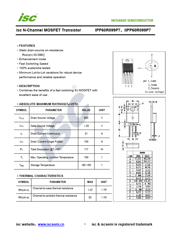
Description
bines the benefits of a fast switching SJ MOSFET with excellent ease of use - SYMBOL PARAMETER VALUE VDSS Drain-Source Voltage 600 VGS Gate-Source Voltage ±20 ID Drain Current-Continuous 31 IDM Drain Current-Single Pulsed 100 PD Total Dissipation @TC=25℃ 117 Tj Max. Operating Junction Temperature 150 Tstg Storage Temperature -55~150 UNIT V V A A W ℃ ℃ - SYMBOL PARAMETER Rth(ch-c) Channel-to-case Rth(ch-a) Channel-to-ambient MAX 1.07 62 UNIT ℃/W ℃/W isc website:.iscsemi.cn 1 isc & iscsemi is registered trademark isc N-Channel MOSFET Transistor IPP60R099P7,IIPP60R099P7 TC=25℃ unless otherwise specified SYMBOL PARAMETER CONDITIONS BVDSS Drain-Source Breakdown Voltage VGS=0V; ID =1mA VGS(th) Gate Threshold Voltage VDS=VGS; ID =0.53mA RDS(on) Drain-Source On-Resistance VGS=10V; ID=10.5A IGSS Gate-Source Leakage Current VGS=20V; VDS=0V IDSS Drain-Source Leakage Current VDS=600V; VGS= 0V VSD Diode forward voltage IF=10.5A; VGS = 0V MIN TYP MAX UNIT 600 V 3 4 V 0.099 Ω 0.1 μA 1 μA 0.9 V NOTICE: ISC reserves the rights to make changes of the content herein the datasheet at any time without notification.
Key Features
- Static drain-source on-resistance: RDS(on) ≤0.099Ω
- Enhancement mode
- Fast Switching Speed
- 100% avalanche tested
- Minimum Lot-to-Lot variations for robust device performance and reliable operation