Datasheet Summary
IS61NLF25672/IS61NVF25672 IS61NLF51236/IS61NVF51236
IS61NLF102418/IS61NVF102418
256K x 72, 512K x 36 and 1M x 18
NOVEMBER 2013
18Mb, FLOW THROUGH 'NO WAIT' STATE BUS SRAM
Features
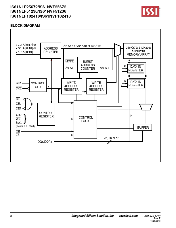
DESCRIPTION
- 100 percent bus utilization
- No wait cycles between Read and Write
- Internal self-timed write cycle
- Individual Byte Write Control
- Single Read/Write control pin
- Clock controlled, registered address, data and control
- Interleaved or linear burst sequence control us- ing MODE input
- Three chip enables for simple depth expansion and address pipelining
- Power Down mode
- mon data inputs and data outputs
- CKE pin to enable clock and suspend operation
- JEDEC 100-pin TQFP, 165-ball...