z z
Maximum Ratings 150 150 ± 20 ± 30 150 75 340 60 80 2.5 10 V V
G
V V A A A A mJ J V/ns
G D
D
S
(TAB)
TO-264(SP) (IXTK)
D (TAB) S D = Drain TAB = Drain
G = Gate S = Source
1.13/10 Nm/lb. in. 5.5 10 g g
z
International standard packages Unclamped Inductive Switching (UIS) rated Low package inductance - easy to drive and to protect
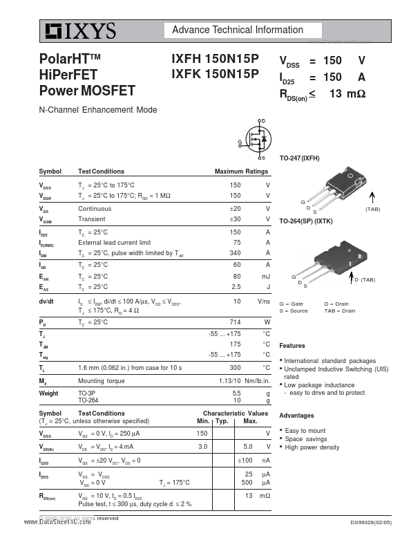
Symbol Test Conditions (TJ = 25°C, unless otherwise specified) VDSS VGS(th) IGSS IDSS RDS(on) VGS = 0 V, ID = 250 µA VDS = VGS, ID = 4 mA VGS = ±20 VDC, VD.
Full PDF Text Transcription for IXFK150N15P (Reference)
Note: Below is a high-fidelity text extraction (approx. 800 characters) for
IXFK150N15P. For precise diagrams, and layout, please refer to the original PDF.
Advance Technical Information www.DataSheet4U.com PolarHTTM HiPerFET Power MOSFET N-Channel Enhancement Mode IXFH 150N15P IXFK 150N15P VDSS = 150 V ID25 = 150 A RDS(on) ≤...
View more extracted text
ent Mode IXFH 150N15P IXFK 150N15P VDSS = 150 V ID25 = 150 A RDS(on) ≤ 13 mΩ TO-247 (IXFH) Symbol VDSS VDGR VGS VGSM ID25 ID(RMS) IDM IAR EAR EAS dv/dt PD TJ TJM Tstg TL Md Weight 1.6 mm (0.062 in.) from case for 10 s Mounting torque TO-3P TO-264 Test Conditions TJ = 25°C to 175°C TJ = 25°C to 175°C; RGS = 1 MΩ Continuous Transient TC = 25°C External lead current limit TC = 25°C, pulse width limited by TJM TC = 25°C TC = 25°C TC = 25°C IS ≤ IDM, di/dt ≤ 100 A/µs, VDD ≤ VDSS, TJ ≤ 175°C, RG = 4 Ω TC = 25°C 714 -55 ... +175 175 -55 ... +175 300 W °C °C °C °C Features z z Maximum Ratings 150 150 ± 20 ± 30 150 75 340 60 80 2.