The following content is an automatically extracted verbatim text
from the original manufacturer datasheet and is provided for reference purposes only.
View original datasheet text
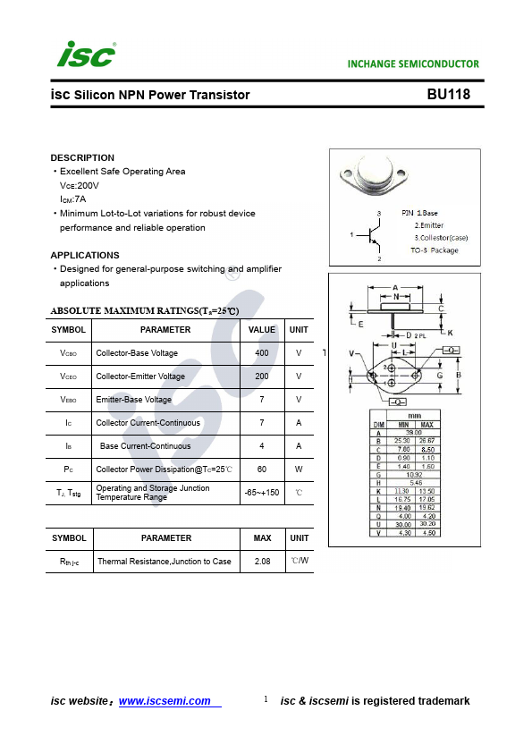
isc Silicon NPN Power Transistor
BU118
DESCRIPTION ·Excellent Safe Operating Area
VCE:200V ICM:7A ·Minimum Lot-to-Lot variations for robust device performance and reliable operation
APPLICATIONS ·Designed for general-purpose switching and amplifier
applications
ABSOLUTE MAXIMUM RATINGS(Ta=25℃)
SYMBOL
PARAMETER
VALUE
UNIT
VCBO
Collector-Base Voltage
400
V THERMAL CHARACTERISTICS
VCEO Collector-Emitter Voltage
200
V
VEBO
Emitter-Base Voltage
7
V
IC
Collector Current-Continuous
7
A
IB
Base Current-Continuous
4
A
PC
Collector Power Dissipation@TC=25℃
60
W
TJ, Tstg
Operating and Storage Junction Temperature Range
-65~+150 ℃
SYMBOL
PARAMETER
Rth j-c Thermal Resistance,Junction to Case
MAX 2.08
UNIT ℃/W
isc website:www.iscsemi.