IKW50N65SS5
Features
- VCE = 650 V
- IC = 50 A
- Ultra-low switching losses due to the bination of TRENCHSTOPTM 5 and Cool Si CTM technology
- Very low on-state losses
- Benchmark efficiency in hard switching topologies
- Plug-and-play replacement of pure silicon devices
- Maximum junction temperature Tvjmax = 175°C
- Qualified according to JEDEC for target applications
- Pb-free lead plating; Ro HS pliant
- plete product spectrum and PSpice Models: http://.infineon./igbt/ Potential applications
- Industrial SMPS
- Industrial UPS
- Solar string inverter
- Energy storage
- Charger Product validation
- Qualified for applications listed above based on the test conditions in the relevant tests of
JEDEC20/22 Description
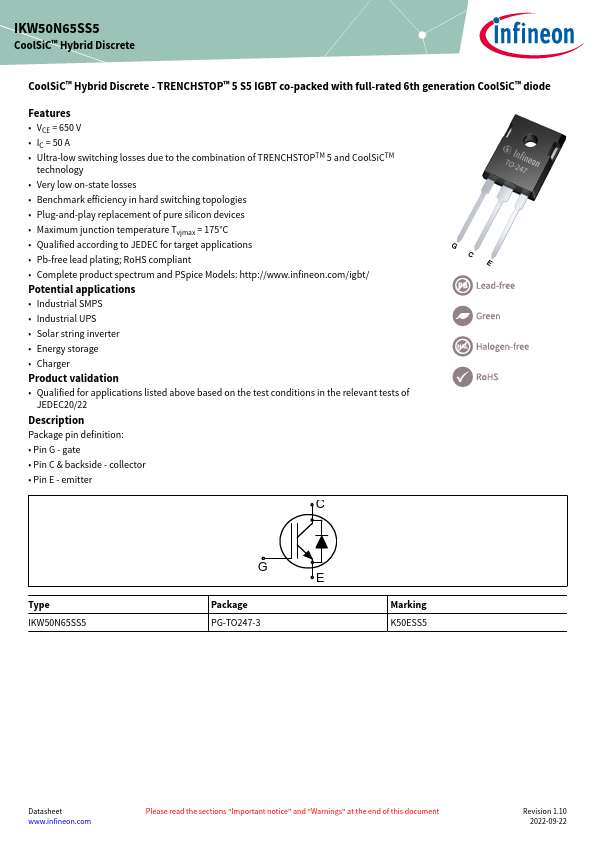
Package pin definition:
- Pin G
- gate
- Pin C & backside
- collector
- Pin E
- emitter
TO-247
- 3Pin
2021-10-27 restricted
Copyright © Infineon T
Type IKW50N65SS5
Package PG-TO247-3
Marking K50ESS5
Datasheet .infineon.
Please read the sections "Important notice" and...