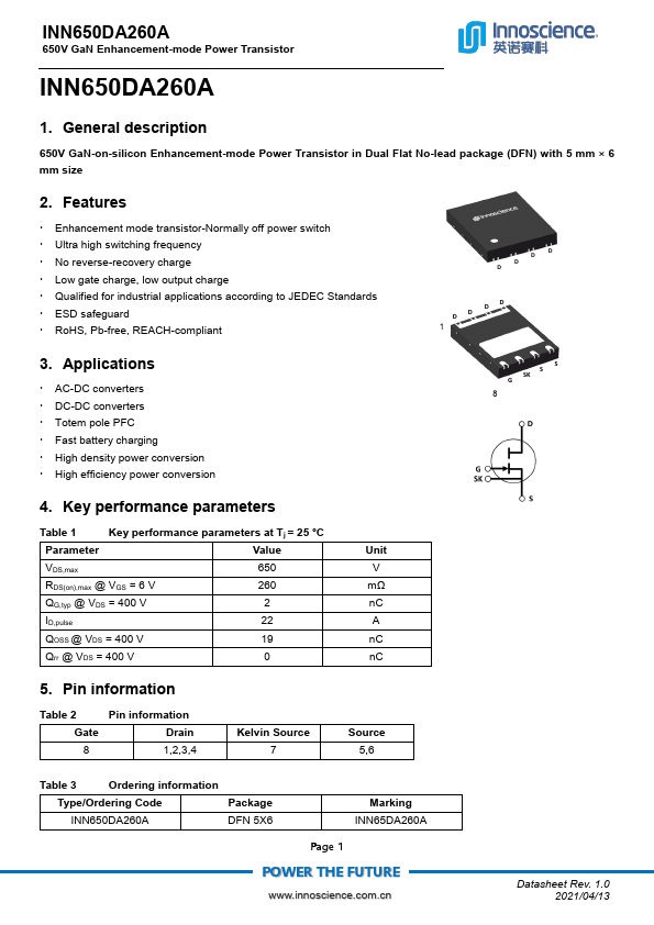
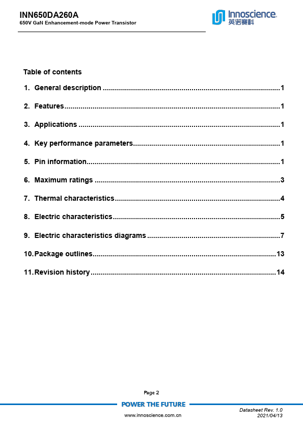
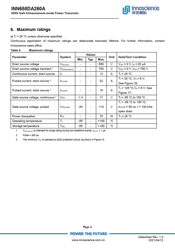
FEATURES
Enhancement mode transistor-Normally off power switch Ultra high switching frequency No reverse-recovery charge Low gate charge, low output charge Qualified for industrial applications according to JEDEC Standards ESD safeguard RoHS, Pb-free, REACH-compliant DD D D DD D D 1 3. APPLICATIONS
AC-DC converters DC-DC converters Totem pole PFC Fast battery charging High density power conversion High efficiency power conversion S S SK G 8 4. Key performance parameters Table 1 Key performance parameters at Tj = 25 °C Parameter Value VDS,max 650 RDS(on),max @ VGS = 6 V 260 QG,typ @ VDS = 400 V 2 ID,pulse 22 QOSS @ VDS = 400 V 19 Qrr @ VDS = 400 V 0 Unit V mΩ nC A nC nC 5. Pin information Table 2 Pin information Gate Drain 8 1,2,3,4 Kelvin Source 7 Source 5,6 Table 3 Ordering information Type/Ordering Code Package INN650DA260A DFN 5X6 Marking INN65DA260A Page 1 POWER THE FUTURE Datasheet Rev. 1.0 2021/04/13 INN650DA260A 650V GaN Enhancement-mode Power Transistor Table of contents 1.