Datasheet4U Logo Datasheet4U.com

ICSSSTV16859 - DDR 13-Bit to 26-Bit Registered Buffer

Datasheet Summary

Description

The 13-bit to 26-bit ICSSTV16859 is a universal bus driver designed for 2.3V to 2.7V VDD operation and SSTL_2 I/O Levels except for the RESET# input which is LVCMOS.

Data flow from D to Q is controlled by the differential clock, CLK, CLK# and RESET#.

Data is triggered on the positive edge of CLK.

Features

  • Differential clock signals.
  • Meets SSTL_2 signal data.
  • Supports SSTL_2 class II specifications on outputs.
  • low-voltage operation - VDD = 2.3V to 2.7V.
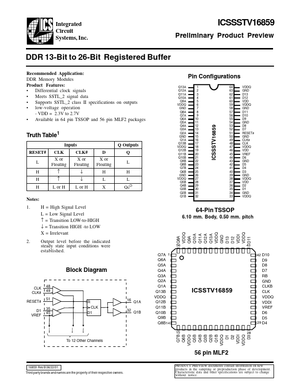
  • Available in 64 pin TSSOP and 56 pin MLF2 packages Pin Configurations Q13A Q12A Q11A Q10A Q9A VDDQ GND Q8A Q7A Q6A Q5A Q4A Q3A Q2A GND Q1A Q13B VDDQ Q12B Q11B Q10B Q9B Q8B Q7B Q6B GND VDDQ Q5B Q4B Q3B Q2B Q1B 1 2 3 4 5 6 7 8 9 10 11 12 13 14 15 16 17 18 19 20 21 22 23 24 25 26 27 28 29 30 31 32 64 63.

📥 Download Datasheet

Datasheet preview – ICSSSTV16859

Datasheet Details

Part number ICSSSTV16859
Manufacturer Integrated Circuit Systems
File Size 233.84 KB
Description DDR 13-Bit to 26-Bit Registered Buffer
Datasheet download datasheet ICSSSTV16859 Datasheet
Additional preview pages of the ICSSSTV16859 datasheet.
Other Datasheets by Integrated Circuit Systems

Full PDF Text Transcription

Click to expand full text
Integrated Circuit Systems, Inc. ICSSSTV16859 Preliminary Product Preview DDR 13-Bit to 26-Bit Registered Buffer Recommended Application: DDR Memory Modules Product Features: • Differential clock signals • Meets SSTL_2 signal data • Supports SSTL_2 class II specifications on outputs • low-voltage operation - VDD = 2.3V to 2.
Published: |