ICS8305I Overview
Description
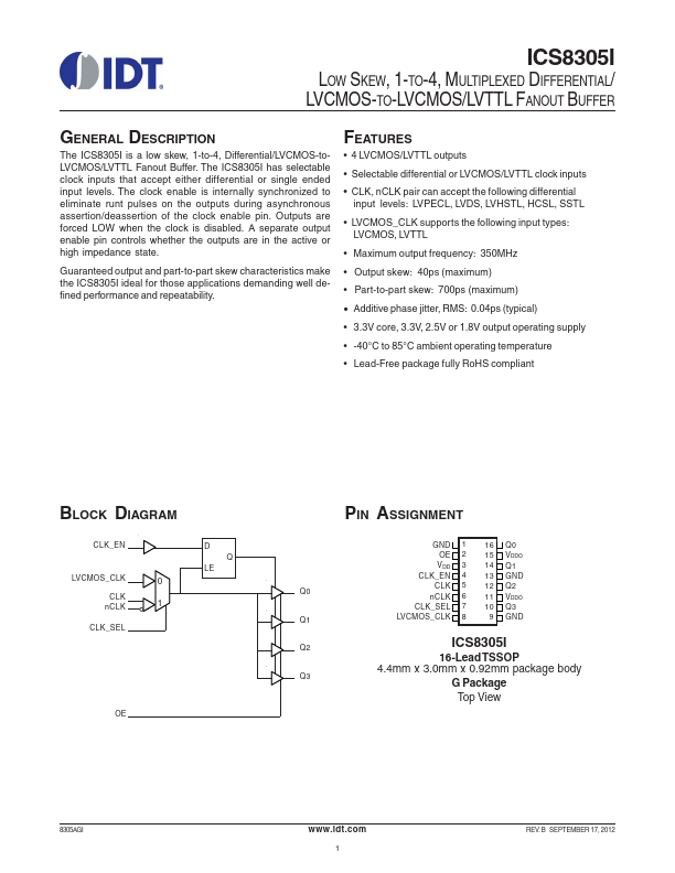
The ICS8305I is a low skew, 1-to-4, Differential/LVCMOS-toLVCMOS/LVTTL Fanout Buffer. The ICS8305I has selectable clock inputs that accept either differential or single ended input levels.
Key Features
- 4 LVCMOS/LVTTL outputs
- Selectable differential or LVCMOS/LVTTL clock inputs
- CLK, nCLK pair can accept the following differential input levels: LVPECL, LVDS, LVHSTL, HCSL, SSTL
- LVCMOS_CLK supports the following input types: LVCMOS, LVTTL
- Maximum output frequency: 350MHz
- Output skew: 40ps (maximum)
- Part-to-part skew: 700ps (maximum)
- Additive phase jitter, RMS: 0.04ps (typical)
- 3.3V core, 3.3V, 2.5V or 1.8V output operating supply
- 40°C to 85°C ambient operating temperature