IDT5V2528
IDT5V2528 is 2.5V / 3.3V PHASE-LOCK LOOP CLOCK DRIVER ZERO DELAY BUFFER manufactured by Integrated Device.
IDT5V2528/A 2.5 / 3.3V PHASE-LOCK LOOP CLOCK DRIVER
2.5V / 3.3V PHASE-LOCK LOOP CLOCK DRIVER ZERO DELAY BUFFER
INDUSTRIALTEMPERATURERANGE
IDT5V2528/A
Features
:
- Operates at 3.3V VDD/AVDD and 2.5V/3.3V VDDQ
- 1:10 fanout
- 3-level inputs for output control
- External feedback (FBIN) pin is used to synchronize the outputs to the clock input signal
- No external RC network required for PLL loop stability
- Configurable 2.5V or 3.3V LVTTL outputs
- t PD Phase Error at 100MHz to 166MHz: ±150ps
- Jitter (peak-to-peak) at 133MHz and 166MHz: ±75ps
- Spread spectrum patible
- Operating Frequency:
- Std: 25MHz to 140MHz
- A: 25MHz to 167MHz
- Available in TSSOP package
DESCRIPTION:
The IDT5V2528 is a high performance, low-skew, low-jitter, phase-lock loop (PLL) clock driver. It uses a PLL to precisely align, in both frequency and phase, the feedback (FBOUT) output to the clock (CLK) input signal.
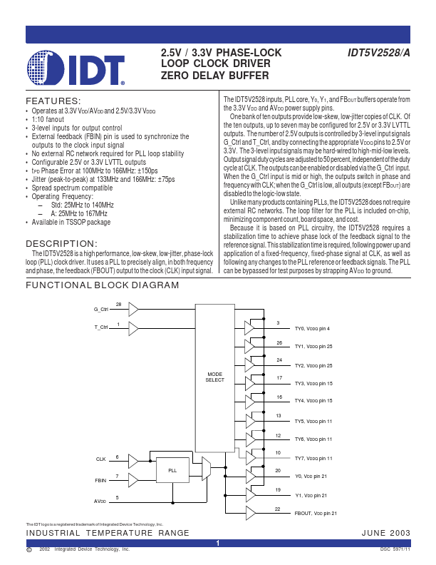
FUNCTIONAL BLOCK DIAGRAM
The IDT5V2528 inputs, PLL core, Y0, Y1, and FBOUT buffers operate from the 3.3V VDD and AVDD power supply pins.
One bank of ten outputs provide low-skew, low-jitter copies of CLK. Of the ten outputs, up to seven may be configured for 2.5V or 3.3V LVTTL outputs. The number of 2.5V outputs is controlled by 3-level input signals G_Ctrl and T_Ctrl, and by connecting the appropriate VDDQ pins to 2.5V or 3.3V. The 3-level input signals may be hard-wired to high-mid-low levels. Output signal duty cycles are adjusted to 50 percent, independent of the duty cycle at CLK. The outputs can be enabled or disabled via the G_Ctrl input. When the G_Ctrl input is mid or high, the outputs switch in phase and frequency with CLK; when the G_Ctrl is low, all outputs (except FBOUT) are disabled to the logic-low state.
Unlike many products containing PLLs, the IDT5V2528 does not require external RC networks. The loop filter for the PLL is included on-chip, minimizing ponent count, board space, and cost.
Because it is based on PLL circuitry, the IDT5V2528 requires a...