IS41LV16100B
IS41LV16100B is 1M x 16 DYNAMIC RAM WITH EDO PAGE MODE manufactured by ISSI.
FEATURES
- TTL patible inputs and outputs; tristate I/O
- Refresh Interval:
- Auto refresh Mode: 1,024 cycles /16 ms
- RAS-Only, CAS-before-RAS (CBR), and Hidden
- JEDEC standard pinout
- Single power supply: 3.3V ± 10%
- Byte Write and Byte Read operation via two CAS
- Industrial Temperature Range: -40o C to +85o C
- Lead-free available
..
ISSI
APRIL 2005
®
DESCRIPTION
The ISSI IS41LV16100B is 1,048,576 x 16-bit high-performance CMOS Dynamic Random Access Memories. These devices offer an accelerated cycle access called EDO Page Mode. EDO Page Mode allows 1,024 random accesses within a single row with access cycle time as short as 20 ns per 16-bit word. These features make the IS41LV16100B ideally suited for high-bandwidth graphics, digital signal processing, highperformance puting systems, and peripheral applications. The IS41LV16100B is packaged in a 42-pin 400-mil SOJ and 400-mil 50- (44-) pin TSOP (Type II).
KEY TIMING PARAMETERS
Parameter -50 50 14 25 30 85 -60 60 15 30 40 110 Unit ns ns ns ns ns
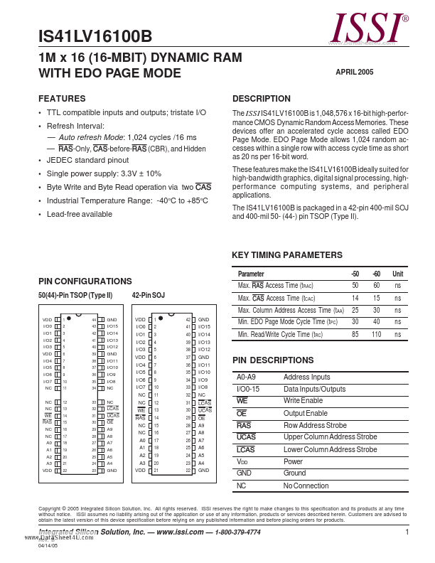
PIN CONFIGURATIONS
50(44)-Pin TSOP (Type II) 42-Pin SOJ
Max. RAS Access Time (t RAC) Max. CAS Access Time (t CAC) Max. Column Address Access Time (t AA)
42 41 40 39 38 37 36 35 34 33 32 31 30 29 28 27 26 25 24 23 22 GND I/O15 I/O14 I/O13 I/O12 GND I/O11 I/O10 I/O9 I/O8 NC LCAS UCAS OE A9 A8 A7 A6 A5 A4 GND
VDD I/O0 I/O1 I/O2 I/O3 VDD I/O4 I/O5 I/O6 I/O7 NC NC NC WE RAS NC NC A0 A1 A2 A3 VDD
1 2 3 4 5 6 7 8 9 10 11 12 13 14 15 16 17 18 19 20 21 22
44 43 42 41 40 39 38 37 36 35 34 33 32 31 30 29 28 27 26 25 24 23
GND I/O15 I/O14 I/O13 I/O12 GND I/O11 I/O10 I/O9 I/O8 NC NC LCAS UCAS OE A9 A8 A7 A6 A5 A4 GND
VDD I/O0 I/O1 I/O2 I/O3 VDD I/O4 I/O5 I/O6 I/O7 NC NC WE RAS NC NC A0 A1 A2 A3 VDD
1 2 3 4 5 6 7 8 9 10 11 12 13 14 15 16 17 18 19 20 21
Min. EDO Page Mode Cycle Time (t PC) Min. Read/Write Cycle Time (t RC)
PIN DESCRIPTIONS
A0-A9 I/O0-15 WE OE RAS UCAS LCAS VDD GND NC Address Inputs Data Inputs/Outputs Write Enable Output Enable Row Address Strobe Upper...