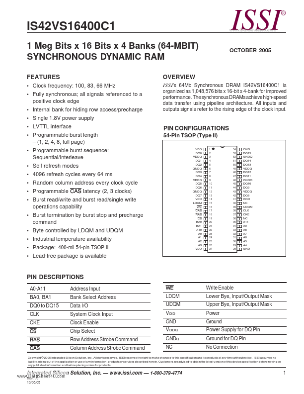
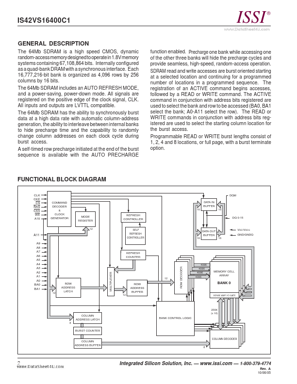
Datasheet4U Logo Datasheet4U.com

IS42VS16400C1 - 1 Meg Bits x 16 Bits x 4 Banks (64-MBIT) SYNCHRONOUS DYNAMIC RAM

General Description

A0-A11 BA0, BA1 DQ0 to DQ15 CLK CKE CS RAS CAS Address Input Bank Select Address Data I/O System Clock Input Clock Enable Chip Select Row Address Strobe Command Column Address Strobe Command WE LDQM UDQM VDD GND VDDQ GNDQ NC Write Enable Lower Bye, Input/Output Mask Upper Bye, Input/Output Mask Pow

Key Features

  • Clock frequency: 100, 83, 66 MHz.
  • Fully synchronous; all signals referenced to a positive clock edge.
  • Internal bank for hiding row access/precharge.
  • Single 1.8V power supply.
  • LVTTL interface.
  • Programmable burst length.
  • (1, 2, 4, 8, full page).
  • Programmable burst sequence: Sequential/Interleave.
  • Self refresh modes.
  • 4096 refresh cycles every 64 ms.
  • Random column address every clock cycle.
  • P.

📥 Download Datasheet

Full PDF Text Transcription for IS42VS16400C1 (Reference)

Note: Below is a high-fidelity text extraction (approx. 800 characters) for IS42VS16400C1. For precise diagrams, and layout, please refer to the original PDF.

IS42VS16400C1 1 Meg Bits x 16 Bits x 4 Banks (64-MBIT) SYNCHRONOUS DYNAMIC RAM FEATURES • Clock frequency: 100, 83, 66 MHz • Fully synchronous; all signals referenced to ...

View more extracted text
uency: 100, 83, 66 MHz • Fully synchronous; all signals referenced to a positive clock edge • Internal bank for hiding row access/precharge • Single 1.8V power supply • LVTTL interface • Programmable burst length – (1, 2, 4, 8, full page) • Programmable burst sequence: Sequential/Interleave • Self refresh modes • 4096 refresh cycles every 64 ms • Random column address every clock cycle • Programmable CAS latency (2, 3 clocks) • Burst read/write and burst read/single write operations capability • Burst termination by burst stop and precharge command • Byte controlled by LDQM and UDQM • Industrial temperature availability •