J113A
Description
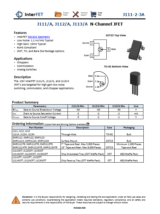
The -25V InterFET J111/A, J112/A, and J113/A JFET’s are targeted for high gain low noise switching, commutator, and chopper applications. Source 1 Drain 2 Gate 3 Drain 2 Source 1 SOT23 Top View 3 Gate TO-92 Bottom View Product Summary Parameters BVGSS Gate to Source Breakdown Voltage IDSS Drain to Source Saturation Current VGS(off) Gate to Source Cutoff Voltage J111/A Min J112/A Min J113/A Min Unit -40 -40 -40 V -2 -2 -2 mA -5 -2 -1 V.
Key Features
- InterFET N0132S Geometry
- Low Noise: 1.2 nV/√Hz Typical
- High Gain: 15mS Typical
- RoHS Compliant
- SMT, TH, and Bare Die Package options.