IRF8113
IRF8113 is Power MOSFET manufactured by International Rectifier.
- 94637A
HEXFET® Power MOSFET
Applications l Synchronous MOSFET for Notebook Processor Power l Synchronous Rectifier MOSFET for
Isolated DC-DC Converters in Networking Systems Benefits l Very Low RDS(on) at 4.5V VGS l Low Gate Charge l Fully Characterized Avalanche Voltage and Current
VDSS
RDS(on) max
Qg Typ. 24n C
30V 5.6m:@VGS = 10V
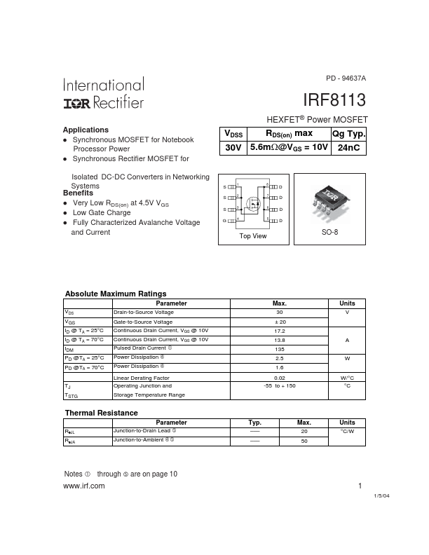
A A D D D D
Top View
SO-8
Absolute Maximum Ratings
Parameter
VDS VGS ID @ TA = 25°C ID @ TA = 70°C IDM PD @TA = 25°C PD @TA = 70°C TJ TSTG Drain-to-Source Voltage Gate-to-Source Voltage Continuous Drain Current, VGS @ 10V Continuous Drain Current, VGS @ 10V Pulsed Drain Current Power Dissipation Power Dissipation
Max.
30 ± 20 17.2 13.8 135 2.5 1.6 0.02 -55 to + 150
Units
V f f c
Linear Derating Factor Operating Junction and Storage Temperature Range
W/°C °C
Thermal Resistance
RθJL RθJA g Junction-to-Ambient fg
Junction-to-Drain Lead
Parameter
Typ.
- -
- -
- -
Max.
20...