CD4075BMS Overview
Description
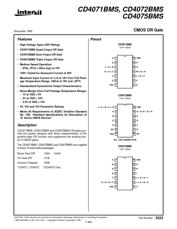
CD4071BMS, CD4072BMS and CD4075BMS OR gates provide the system designer with direct implementation of the positive-logic OR function and supplement the existing family of CMOS gates. The CD4071BMS, CD4072BMS and CD4075BMS are supplied in these 14 lead outline packages: Braze Seal DIP Frit Seal DIP Ceramic Flatpack *CD4071, CD4072 *H4H H1B H3W †CD4075 Only †H4Q D 5 NC 6 VSS 7 NC = NO CONNECTION CD4075BMS TOP VIEW A 1 B 2 D 3 E 4 F 5 K=D+E+F 6 VSS 7 14 VDD 13 G 12 H 11 I 10 L = G + H + I 9 J=A+B+C 8 C CAUTION: These devices are sensitive to electrostatic discharge; follow proper IC Handling Procedures.
Key Features
- High-Voltage Types (20V Rating)
- CD4071BMS Quad 2-Input OR Gate
- CD4072BMS Dual 4-Input OR Gate
- CD4075BMS Triple 3-Input OR Gate
- Medium Speed Operation