JCET 2N7002T
N-Channel MOSFET
| Part No. | 2N7002T |
|---|---|
| Datasheet | 2N7002T Download |
| Manufacturer |  JCET |
| Description | N-Channel MOSFET |
| Buy | Stock & Price |
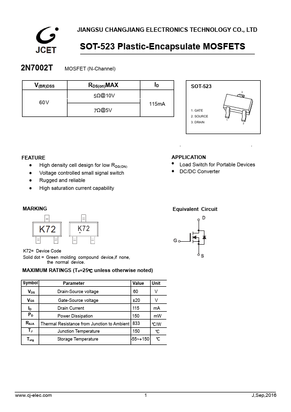
MAXIMUM RATINGS
(Ta=25℃ unless otherwise noted) Symbol Parameter Value Unit VDS Drain-Source voltage 60 V VGS Gate-Source voltage ±20 V ID Drain Current PD Power Dissipation 115 mA 150 mW RθJA Thermal Resistance from Junction to Ambient 833 TJ Junction Temperature 150 ℃/W ℃ Tstg Storage Temperature -55~+150 ℃ 1 J,Sep,2016 MOSFETELECTRICAL CHARACTERISTICS
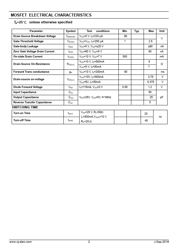
Ta=25 ℃ unless otherwise specified Parameter Drain-Source Breakdown Voltage Gate-Threshold Voltage Gate-body Leakage Zero Gate Voltage Drain Current On-state Drain Current Drain-Source On-Resistance Forward Trans conductance Drain-source on-voltage Diode Forward Voltage Input Capacitance Output Capacitance Reverse Transfer Capacitance SWITCHING TIME Turn-on Time Turn-off Time Symbol V(BR)DSS Vth(GS) lGSS IDSS ID(ON) RDS(on) gfs VDS(on) VSD Ciss Coss Crss Test conditions VGS=0 V, ID=250 µA VDS=VGS, ID=250 µA VDS=0 V, VGS=±20 V VDS=60 V, VGS=0 V VGS=10 V, VDS=7 V VGS=10 V, ID=500mA VGS=5 V, ID=50mA VDS=10 V, ID=200mA VGS=10V, ID=500mA V...