GENERAL DESCRIPTION
FEATURES
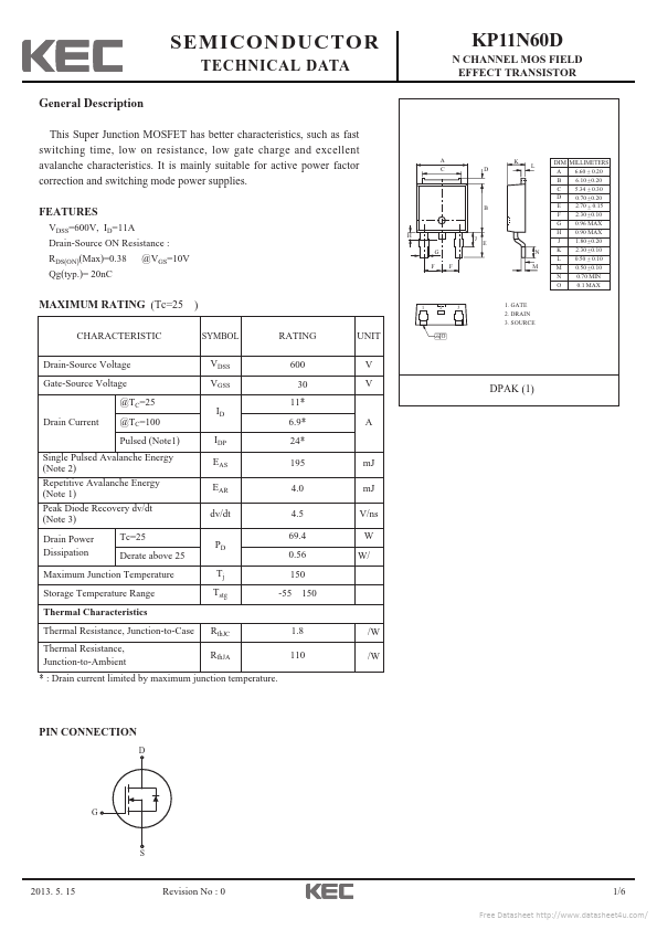
VDSS=600V, ID=11A Drain-Source ON Resistance : G H KP11N60D N CHANNEL MOS FIELD EFFECT TRANSISTOR A C K D L B J E N RDS(ON)(Max)=0.38 Qg(typ.)= 20nC @VGS=10V F F M DIM MILLIMETERS _ 0.20 A 6.60 + _ 0.20 6.10 + B _ 0.30 5.34 + C _ 0.20 D 0.70 + _ 0.15 E 2.70 + _ 0.10 2.30 + F 0.96 MAX G 0.90 MAX H _ 0.20 1.80 + J _ 0.10 2.30 + K _ 0.10 0.50 + L _ 0.10 M 0.50 + 0.70 MIN N 0.1 MAX O MAXIMUM RATING (Tc=25 CHARACTERISTIC Drain-Source Voltage Gate-Source Voltage @TC=25 Drain Current @TC=100 Pulsed (Note1) Single Pulsed Avalanche Energy (Note 2) Repetitive Avalanche Energy (Note 1) Peak Diode Recovery dv/dt (Note 3) Drain Power Dissipation Tc=25 ) SYMBOL VDSS VGSS ID 6.9* IDP EAS EAR dv/dt PD 24* 195 4.0 4.5 69.4 0.56 Tj Tstg 150 -55 150 mJ mJ V/ns W W/ A RATING 600 30 11* UNIT V V 1 2 3 1. GATE 2. DRAIN 3. SOURCE O DPAK (1) Derate above 25 Maximum Junction Temperature Storage Temperature Range Thermal Characteristics Thermal Resistance, Junction-to-Case Thermal Resistance, Junction-to-Ambient RthJC RthJA 1.8 110 /W /W * : Drain current limited by maximum junction temperature. KEC