KIA 50N03
N-CHANNEL MOSFET
| Part No. | 50N03 |
|---|---|
| Datasheet | 50N03 Download |
| Manufacturer |  KIA |
| Description | N-CHANNEL MOSFET |
| Buy | Stock & Price |

FEATURES
● Advanced trench process technology● High density cell design for ultra low on-resistance
● Fully characterized avalanche voltage and current 2.
APPLICATIONS
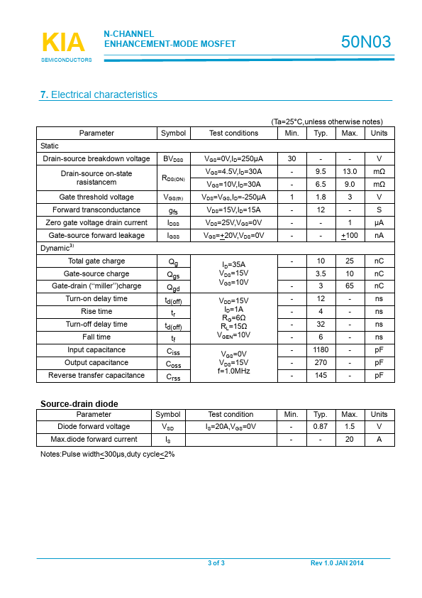
● VDSS=30V,RDS(on)=6.5mΩ,ID=50A● Vds=30V
● RDS(ON)=6.5mΩ(Max.),VGS@10V,Ids@30A
● RDS(ON)=9.5mΩ(Max.),VGS@4.5V,Ids@30A 3. Pin configuration 50N03 Pin Function 1 Gate 2 Drain 3 Source 4 Drain 1 of 3 Rev 1.0 JAN 2014 KIA SEMICONDUCTORS N-CHANNEL ENHANCEMENT-MODE MOSFET 50N03 4. Maximum ratings and thermal characteristics Rating Drain-source voltage Gate-source voltage Continuous drain current Pulsed drain current1) Maximum power dissipation TA=25°C TA=75°C Operating junction and storage temperature range Junction-to-case thermal resistance Junction-to ambient themal rasistance (PCB mount)2) (Ta=25°C,unless otherwise notes) Symbol Value Unit VDS 30 V VGS +20 V ID 50 A IDM 200 A PD 60 W PD TJ/TSTG 23 -55 to 150 W °C RθJC 1.8 °C/W RθJA 50 °C/W Note:1.Repetitive rating:pulse width limited by the maximum junction temperation 2.1-in2 2oz Cu PCB board 3.Guaranteed by design;not subject to production testing 5.