DESCRIPTION
FEATURES
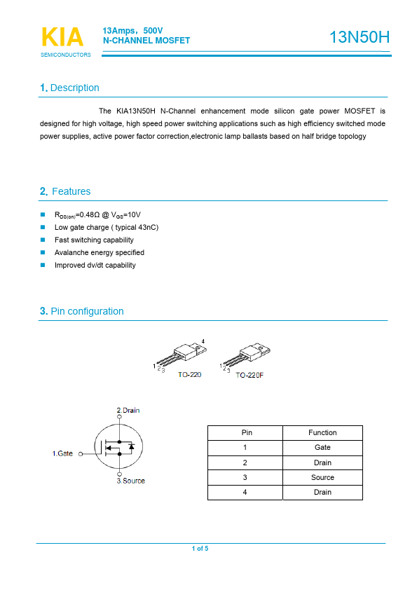
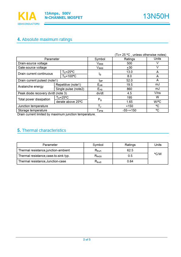
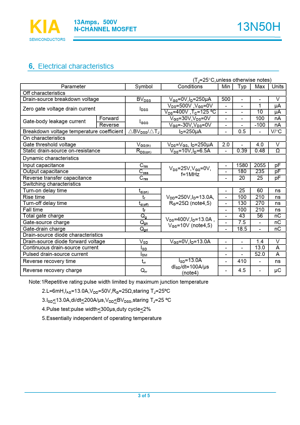
RDS(on)=0.48Ω @ VGS=10V Low gate charge ( typical 43nC) Fast switching capability Avalanche energy specified Improved dv/dt capability 3. Pin configuration Pin 1 2 3 4 1 of 5 Function Gate Drain Source Drain KIA SEMICONDUCTORS 13Amps,500V N-CHANNEL MOSFET 13N50H 4. Absolute maximum ratings Parameter Symbol Drain-source voltage Gate-source voltage Drain current continuous Drain current pulsed (note1) TC=25ºC TC=100ºC Avalanche energy Repetitive (note1) Single pulse (note2) Peak diode recovery dv/dt (note 3) VDSS VGSS ID IDP EAR EAS dv/dt Total power dissipation TC=25ºC derate above 25ºC PD Junction temperature TJ Storage temperature TSTG Drain current limited by maximum junction temperature. (TC= 25 ºC , unless otherwise notes) Ratings Units 500 V +30 V 13.0 A 8.0 A 52.0 A 19.5 mJ 860 mJ 4.5 V/ns 195 W 1.65 W/ºC +150 ºC -55~+150 ºC 5. Thermal characteristics Parameter Thermal resistance,junction-ambient Thermal resistance,case-to-sink typ. Thermal resistance,Junction-case Symbol RthJA RthCS RthJC Ratings 62.5 0.5 0.64 Units ºC/W 2 of 5 KIA SEMICONDUCTORS 13Amps,500V N-CHANNEL MOSFET 13N50H 6. KIA