KK4042B
KK4042B is High-Voltage Silicon-Gate CMOS manufactured by Kodenshi AUK Group.
..
TECHNICAL DATA
Quad Clocked «D» Latch
High-Voltage Silicon-Gate CMOS
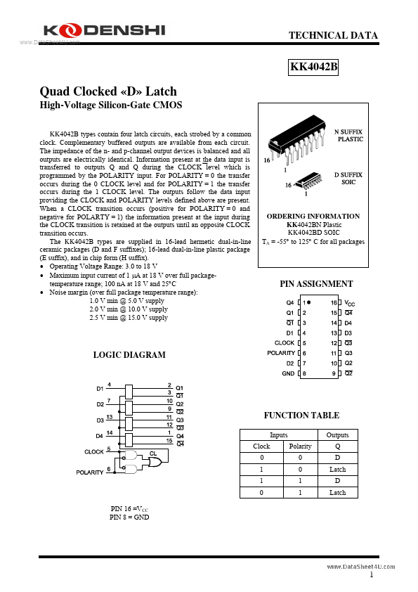
KK4042B types contain four latch circuits, each strobed by a mon clock. plementary buffered outputs are available from each circuit. The impedance of the n- and p-channel output devices is balanced and all outputs are electrically identical. Information present at the data input is transferred to outputs Q and Q during the CLOCK level which is programmed by the POLARITY input. For POLARITY = 0 the transfer occurs during the 0 CLOCK level and for POLARITY = 1 the transfer occurs during the 1 CLOCK level. The outputs follow the data input providing the CLOCK and POLARITY levels defined above are present. When a CLOCK transition occurs (positive for POLARITY = 0 and negative for POLARTY = 1) the information present at the input during the CLOCK transition is retained at the outputs until an opposite CLOCK transition occurs. The KK4042B types are supplied in 16-lead hermetic dual-in-line ceramic packages (D and F suffixes); 16-lead dual-in-line plastic package (E suffix), and in chip form (H suffix).
- Operating Voltage Range: 3.0 to 18 V
- Maximum input current of 1 µA at 18 V over full packagetemperature range; 100 n A at 18 V and 25°C
- Noise margin (over full package temperature range): 1.0 V min @ 5.0 V supply 2.0 V min @ 10.0 V supply 2.5 V min @ 15.0 V supply
ORDERING INFORMATION KK4042BN Plastic KK4042BD SOIC TA = -55° to 125° C for all packages
PIN ASSIGNMENT
LOGIC DIAGRAM
FUNCTION TABLE
Inputs Clock 0 1 1 0 PIN 16 =VCC PIN 8 = GND Polarity 0 0 1 1 Outputs Q D Latch D Latch
..
MAXIMUM RATINGS-
Symbol VCC VI VOUT II PD Ptot Tstg TL
- Parameter DC Supply Voltage (Referenced to GND) DC Input Voltage (Referenced to GND) DC Output Voltage (Referenced to GND) DC Input Current, per Pin Power Dissipation in Still Air, Plastic DIP+ SOIC Package+ Power Dissipation per Output Transistor Storage Temperature Lead Temperature, 1 mm...