KK4049B
KK4049B is Hex Buffer/Converter High-Voltage Silicon-Gate CMOS manufactured by Kodenshi AUK Group.
..
TECHNICAL DATA
Hex Buffer/Converter
High-Voltage Silicon-Gate CMOS
The KK4049B is inverting hex buffers and feature logic-level conversion using only one supply (voltage (VCC). The input-signal high level (VIH) can exceed the VCC supply voltage when these devices are used for logic-level conversions. These devices are intended for use as CMOS to DTL/TTL converters.
- Operating Voltage Range: 3.0 to 18 V
- Maximum input current of 1 µA at 18 V over full package-temperature range; 100 n A at 18 V and 25°C
- Noise margin (over full package temperature range): 0.5 V min @ 5.0 V supply 1.0 V min @ 10.0 V supply 1.0 V min @ 15.0 V supply
- High-to-low level conversion
ORDERING INFORMATION KK4049BN Plastic KK4049BD SOIC TA = -55° to 125° C for all packages
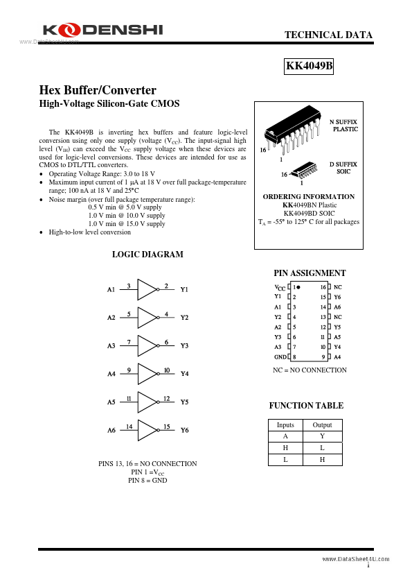
LOGIC DIAGRAM PIN ASSIGNMENT
NC = NO CONNECTION
FUNCTION TABLE
Inputs A H PINS 13, 16 = NO CONNECTION PIN 1 =VCC PIN 8 = GND L Output Y L H
..
MAXIMUM RATINGS-
Symbol VCC VIN VOUT IIN PD PD Tstg TL
- Parameter DC Supply Voltage (Referenced to GND) DC Input Voltage (Referenced to GND) DC Output Voltage (Referenced to GND) DC Input Current, per Pin Power Dissipation in Still Air, Plastic DIP+ SOIC Package+ Power Dissipation per Output Transistor Storage Temperature Lead Temperature, 1 mm from Case for 10 Seconds (Plastic DIP or SOIC Package)
Value -0.5 to +20 VCC-
- to +18 -0.5 to VCC +0.5 ±10 750 500 100 -65 to +150 260
Unit V V V m A m W m W °C °C
Maximum Ratings are those values beyond which damage to the device may occur. Functional operation should be restricted to the Remended Operating Conditions. +Derating
- Plastic DIP:
- 10 m W/°C from 65° to 125°C SOIC Package: :
- 7 m W/°C from 65° to 125°C
- - The KK4049B has high-to-low level voltage conversion capability but not low-to-high level; therefore it is remended that VIN ≥ VCC
REMENDED OPERATING CONDITIONS
Symbol VCC VIN VOUT TA
- -
Parameter DC Supply Voltage (Referenced to GND) DC Input...