KK4051B
KK4051B is Analog Multiplexer Demultiplexer High-Performance Silicon-Gate CMOS manufactured by Kodenshi AUK Group.
..
TECHNICAL DATA
Analog Multiplexer Demultiplexer
High-Performance Silicon-Gate CMOS
The KK4051B analog multiplexer/demultiplexer is digitally controlled analog switches having low ON impedance and very low OFF leakage current. Control of analog signals up to 20V peak-to-peak can be achieved by digital signal amplitudes of 4.5 to 20V (if VCC
- GND = 3V, a VCC
- VEE of up to 13 V can be controlled; for VCC-VEE level differences above 13V a VCC
- GND of at least 4.5V is required). These multiplexer circuits dissipate extremely low quiescent power over the full VCC -GND and VCC
- VEE supply-voltage ranges, independent of the logic state of the control signals. When a logic “1”is present at the ENABLE input terminal all channels are off. The KK4051B is a single 8-channel multiplexer having three binary control inputs, A, B and C, and an ENABLE input. The three binary signals select 1 of 8 channels to be turned on, and connect one of the 8 inputs to the output.
- Operating Voltage Range: 3.0 to 18 V
- Maximum input current of 1 µA at 18 V over full package-temperature range; 100 n A at 18 V and 25°C
- Noise margin (over full package temperature range): 1.0 V min @ 5.0 V supply 2.0 V min @ 10.0 V supply 2.5 V min @ 15.0 V supply
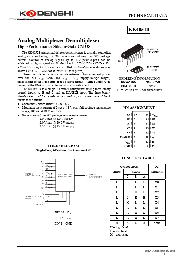
N SUFFIX PLASTIC 16 1 16 1 D SUFFIX SOIC
ORDERING INFORMATION KK4051BN Plastic DIP KK4051BD SOIC TA = -55° to 125° C for all packages
PIN ASSIGNMENT
LOGIC DIAGRAM
Single-Pole, 8-Position Plus mon Off
FUNCTION TABLE
X0 X1 X2 X3 ANALOG INPUTS/OUTPUTS X4 X5 13 14 15 12 1 5 MULTIPLEXER/ DEMULTIPLEXER 3 X MON OUTPUT/INPUT
Control Inputs Enable C L L L L L L PIN 16 =VCC PIN 7 = VEE PIN 8 = GND L L L L L L H H H H Select B L L H H L L H H X A L H L H L H L H X
ON Channels X0 X1 X2 X3 X4 X5 X6 X7 None
X6 2 X7 4
A CHANNEL-SELECT B INPUTS C ENABLE
11 10 9 6
H X H = high level L = low level X = don’t care
..
MAXIMUM RATINGS-
Symbol VCC VIN IIN PD Ptot Tstg TL Parameter DC Supply...