KK4053B
KK4053B is Analog Multiplexer Demultiplexer High-Performance Silicon-Gate CMOS manufactured by Kodenshi AUK Group.
..
TECHNICAL DATA
Analog Multiplexer Demultiplexer
High-Performance Silicon-Gate CMOS
The KK4053B analog multiplexer/demultiplexer is digitally controlled analog switches having low ON impedance and very low OFF leakage current. Control of analog signals up to 20V peak-to-peak can be achieved by digital signal amplitudes of 4.5 to 20V (if VCC
- GND = 3V, a VCC
- VEE of up to 13 V can be controlled; for VCC
- VEE level differences above 13V a VCC
- GND of at least 4.5V is required). These multiplexer circuits dissipate extremely low quiescent power over the full VCC -GND and VCC
- VEE supply-voltage ranges, independent of the logic state of the control signals. When a logic “1”is present at the ENABLE input terminal all channels are off. The KK4053B is a triple 2-channel multiplexer having three separate digital control inputs, A, B, and C, and an enable input. Each control input selects one of a pair of channels which are connected in a singlepole double-throw configuration.
- Operating Voltage Range: 3.0 to 18 V
- Maximum input current of 1 µA at 18 V over full package-temperature range; 100 n A at 18 V and 25°C
- Noise margin (over full package temperature range): 1.0 V min @ 5.0 V supply 2.0 V min @ 10.0 V supply 2.5 V min @ 15.0 V supply
ORDERING INFORMATION KK4053BN Plastic DIP KK4053BD SOIC TA = -55° to 125° C for all packages
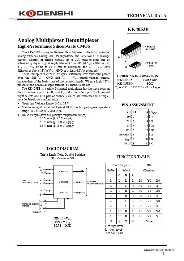
PIN ASSIGNMENT
LOGIC DIAGRAM
Triple Single-Pole, Double-Position Plus mon Off
FUNCTION TABLE
Control Inputs Enable C L L L L L L L L L L L L H H H H Select B L L H H L L H H A L H L H L H L H X Z0 Z0 Z0 Z0 Z1 Z1 Z1 Z1 Y0 Y0 Y1 Y1 Y0 Y0 Y1 Y1 None X0 X1 X0 X1 X0 X1 X0 X1 ON Channels
PIN 16 =VCC PIN 7 = VEE PIN 8 = GND
H X X H = high level L = low level X = don’t care
..
MAXIMUM RATINGS-
Symbol VCC VIN IIN PD Ptot Tstg TL Parameter DC Supply Voltage (Referenced to GND) DC Input Voltage (Referenced to GND) DC Input Current, per Pin Power Dissipation in Still Air Power...