KK74HC4046A
KK74HC4046A is Phase-Locked Loop manufactured by Kodenshi AUK Group.
TECHNICAL DATA
Phase-Locked Loop
High-Performance Silicon-Gate CMOS
The device inputs are patible with standard CMOS outputs; with pullup resistors, they are patible with LS/ALSTTL outputs. The KK74HC4046A phase-locked loop contains three phase parators, a voltage-controlled oscillator (VCO) and unity gain opamp DEMOUT. The parators have two mon signal inputs, PIN, and SIGIN. Input SIGIN and PIN can be used directly coupled to large voltage signals, or indirectly coupled (with a series capacitor to small voltage signals). The self-bias circuit adjusts small voltage signals in the linear region of the amplifier. Phase parator 1 (an exclusive OR gate) provides a digital error signal PC1OUT and maintains 90 degrees phase shift at the center frequency between SIGIN and PIN signals (both at 50% duty cycle). Phase parator 2 (with ORDERING INFORMATION leading-edge sensing logic) provides digital error signals PC2OUT and KK74HC4046AN Plastic PCPOUT and maintains a 0 degree phase shift between SIGIN and PIN KK74HC4046AD SOIC signals (duty cycle is immaterial). The linear VCO produces an output TA = -55° to 125° C for all packages signal VCOOUT whose frequency is determined by the voltage of input VCOIN signal and the capacitor and resistors connected to pins C1A, C1B, R1 and R2. The unity gain op-amp output DEMOUT with an external resistor is used where the VCOIN signal is needed but no loading can be tolerated. The inhibit input, when high, disables the VCO and all on-amps to minimize standby power consumption. Applications include FM and FSK modulation and demodulation, frequency synthesis and multiplication, frequency discrimination, tone decoding, data synchronization and conditioning, voltage-to-frequency conversion and motor speed control.
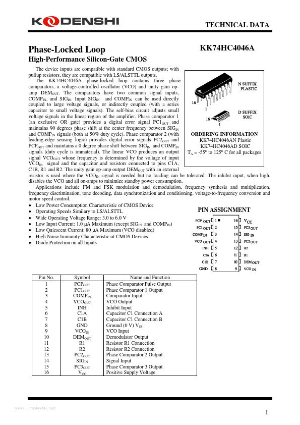
- Low Power Consumption Characteristic of CMOS Device PIN ASSIGNMENT
- Operating Speeds Similary to LS/ALSTTL
- Wide Operating Voltage Range: 3.0 to 6.0 V
- Low Input Current: 1.0 µA...