2SK3483 Overview
Key Features
- Super low on-state resistance: RDS(on)1 = 52m MAX
- (VGS = 10 V, ID = 14A) RDS(on)2 = 59m MAX
- (VGS = 4.5 V, ID = 14A) Low Ciss: Ciss = 2300 pF TYP
| Part | 2SK3483 |
|---|---|
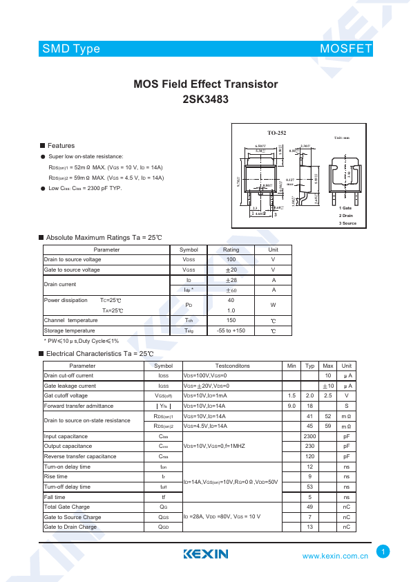
| Description | MOS Field Effect Transistor |
| Category | Transistor |
| Manufacturer | Kexin Semiconductor |
| Size | 42.40 KB |
| Part Number | Manufacturer | Description |
|---|---|---|
| K3483 | NEC | 2SK3483 |
| 2SK3483-ZK | Inchange Semiconductor | N-Channel MOSFET Transistor |
| 2SK3483 | Inchange Semiconductor | N-Channel MOSFET Transistor |
| 2SK3483-Z | Inchange Semiconductor | N-Channel MOSFET Transistor |
| 2SK3483 | NEC | SWITCHING N-CHANNEL POWER MOSFET |