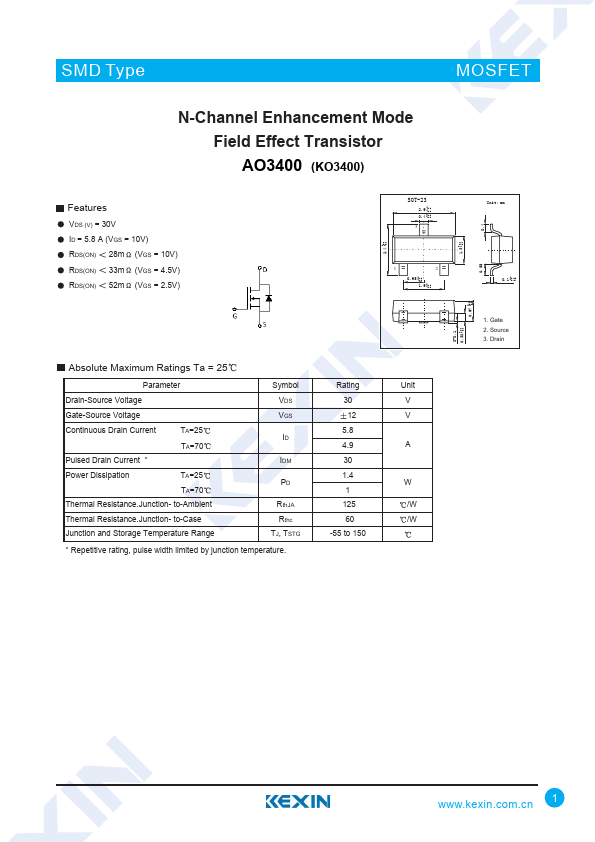
Datasheet4U Logo Datasheet4U.com

AO3400 - N-Channel MOSFET

Key Features

  • VDS (V) = 30V ID = 5.8 A (VGS = 10V) RDS(ON) 28m (VGS = 10V) RDS(ON) 33m (VGS = 4.5V) RDS(ON) 52m (VGS = 2.5V) +0.12.4 -0.1 SOT-23 2.9 +0.1 -0.1 0.4 +0.1 -0.1 3 12 0.95 +0.1 -0.1 1.9 +0.1 -0.1 Absolute Maximum Ratings Ta = 25 Parameter Drain-Source Voltage Gate-Source Voltage Continuous Drain Current TA=25 TA=70 Pulsed Drain Current.
  • Power Dissipation TA=25 TA=70 Thermal Resistance. Junction- to-Ambient Thermal Resistance. Junction- to-Case Junction and Storage Temperature Ran.

📥 Download Datasheet

Full PDF Text Transcription (Reference)

The following content is an automatically extracted verbatim text from the original manufacturer datasheet and is provided for reference purposes only.

View original datasheet text
SMD Type MOSFIECT N-Channel Enhancement Mode Field Effect Transistor AO3400 (KO3400) Features VDS (V) = 30V ID = 5.8 A (VGS = 10V) RDS(ON) 28m (VGS = 10V) RDS(ON) 33m (VGS = 4.5V) RDS(ON) 52m (VGS = 2.5V) +0.12.4 -0.1 SOT-23 2.9 +0.1 -0.1 0.4 +0.1 -0.1 3 12 0.95 +0.1 -0.1 1.9 +0.1 -0.1 Absolute Maximum Ratings Ta = 25 Parameter Drain-Source Voltage Gate-Source Voltage Continuous Drain Current TA=25 TA=70 Pulsed Drain Current * Power Dissipation TA=25 TA=70 Thermal Resistance.Junction- to-Ambient Thermal Resistance.Junction- to-Case Junction and Storage Temperature Range Symbol VDS VGS ID IDM PD RthJA Rthc TJ, TSTG * Repetitive rating, pulse width limited by junction temperature. Rating 30 12 5.8 4.9 30 1.4 1 125 60 -55 to 150 Unit V V A W /W /W 0-0.1 +0.10.38 -0.