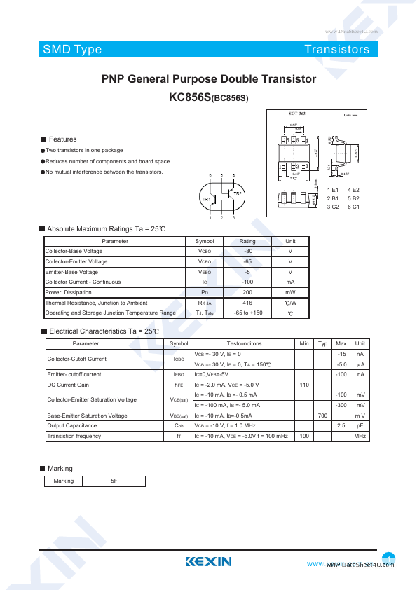
FEATURES
Reduces number of components and board space No mutual interference between the transistors. +0.15 2.3-0.15 0.36 0.1max +0.1 0.3-0.1 +0.1 2.1-0.1 +0.05 0.1-0.02 1 E1 2 B1 3 C2 4 E2 5 B2 6 C1 ABSOLUTE MAXIMUM RATINGS
Ta = 25 Parameter Collector-Base Voltage Collector-Emitter Voltage Emitter-Base Voltage Collector Current - Continuous Power Dissipation Thermal Resistance, Junction to Ambient Operating and Storage Junction Temperature Range Symbol VCBO VCEO VEBO IC PD R JA Rating -80 -65 -5 -100 200 416 -65 to +150 Unit V V V mA mW /W TJ, Tstg ELECTRICAL CHARACTERISTICS
Ta = 25 Parameter Collector-Cutoff Current Emitter- cutoff current DC Current Gain Collector-Emitter Saturation Voltage Base-Emitter Saturation Voltage Output Capacitance Transistion frequency Symbol ICBO IEBO hFE VCE(sat) VBE(sat) Cob fT Testconditons VCB =- 30 V, IE = 0 VCB =- 30 V, IE = 0, TA = 150 IC=0,VEB=-5V IC = -2.0 mA, VCE = -5.0 V IC = -10 mA, IB =- 0.5 mA IC = -100 mA, IB =- 5.0 mA IC = -10 mA, IB=-0.5m...