FDN336P
Key Features
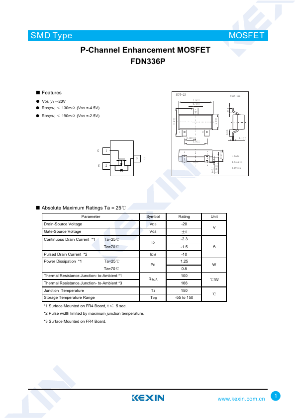
- 9 +0.1 -0.1
- 4 +0.1 -0.1 3 1 2
- 95 +0.1 -0.1 1.9 +0.1 -0.1 +0.1 1.3 -0.1 +0.1 0.97 -0.1
- 4 Unit: mm
- 1 +0.05 -0.01
- Gate 2.Source 3.Drain 0-0.1 +0.1 0.38 -0.1 Ƶ Absolute Maximum Ratings Ta = 25ć Parameter Drain-Source Voltage Gate-Source Voltage Continuous Drain Current *1 Ta=25ć Ta=70ć Pulsed Drain Current *2 Power Dissipation *1 Ta=25ć Ta=70ć Thermal Resistance.Junction- to-Ambient *1 Thermal Resistance.Junction- to-Ambient *3 Junction Temperature Storage Temperature Range Symbol VDS VGS ID IDM PD RthJA TJ Tstg
- 1 Surface Mounted on FR4 Board, t İ 5 sec. *2 Pulse width limited by maximum junction temperature. *3 Surface Mounted on FR4 Board. Rating -20 ±8 -2.3 -1.5 -10 1.25 0.8 100 166 150 -55 to 150 Unit V A W ć/W ć