Datasheet4U Logo Datasheet4U.com

KDS8928A - Dual N & P-Channel Enhancement Mode Field Effect Transistor

Key Features

  • N-Channel 5.5 A, 30 V RDS(ON) = 0.030 @ VGS = 4.5V RDS(ON) = 0.038 @ VGS =2.5V P-Channel -4 A, -20 V RDS(ON) = 0.055 @ VGS =- 4.5 V RDS(ON) = 0.070 @ VGS =-2.5V High density cell design for extremely low RDS(ON). High power and handling capability in a widely used surface mount package Dual (N & P-Channel) MOSFET in surface mount package. Absolute Maximum Ratings Ta = 25 Parameter Drain to Source Voltage Gate to Source Voltage Drain Current Continuous (Note 1a) Drain Current Pulsed Power Dissi.

📥 Download Datasheet

Full PDF Text Transcription (Reference)

The following content is an automatically extracted verbatim text from the original manufacturer datasheet and is provided for reference purposes only.

View original datasheet text
SMD Type TransistIoCrs 
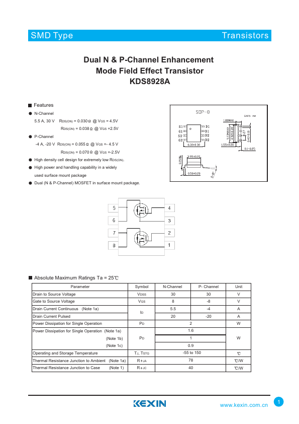
Dual N & P-Channel Enhancement Mode Field Effect Transistor KDS8928A Features N-Channel 5.5 A, 30 V RDS(ON) = 0.030 @ VGS = 4.5V RDS(ON) = 0.038 @ VGS =2.5V P-Channel -4 A, -20 V RDS(ON) = 0.055 @ VGS =- 4.5 V RDS(ON) = 0.070 @ VGS =-2.5V High density cell design for extremely low RDS(ON). High power and handling capability in a widely used surface mount package Dual (N & P-Channel) MOSFET in surface mount package.