SI2303BDS
SI2303BDS is P-Channel Enhancement MOSFET manufactured by Kexin Semiconductor.
SMD Type
P-Channel Enhancement MOSFET SI2303BDS (KI2303BDS)
MOSFET
- Features
- VDS (V) =-30V
- RDS(ON) < 200mΩ (VGS =-10V)
- RDS(ON) < 380mΩ (VGS =-4.5V)
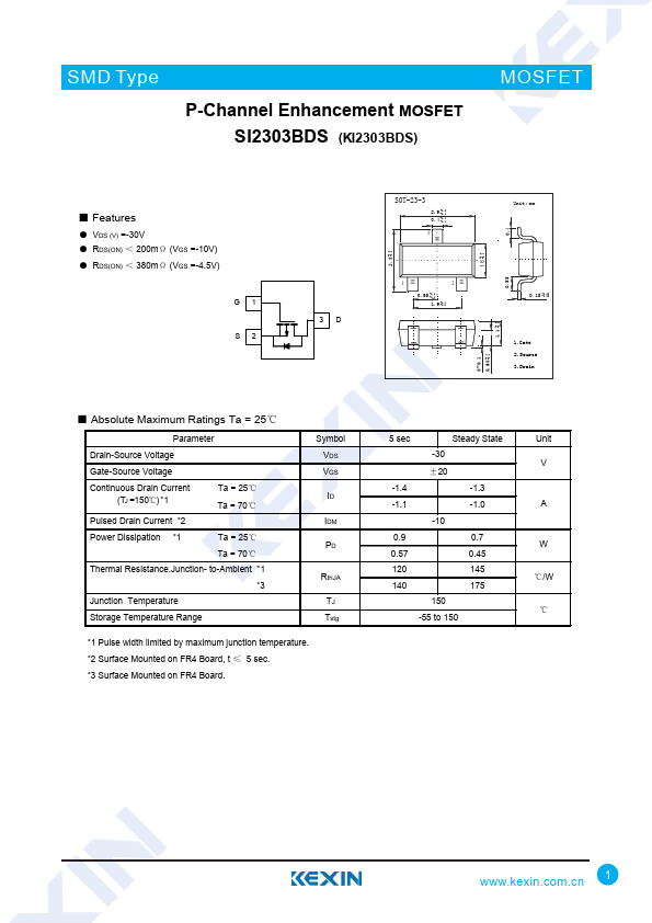
G1
S2
3D
+0.2 2.8 -0.1
SOT-23-3
2.9 +0.2 -0.1
0.4 +0.1 -0.1
0.95 +0.1 -0.1 1.9 +0.1 -0.2
+0.2 1.6 -0.1
+0.2 1.1 -0.1
Unit: mm
0.15 +0.02 -0.02
1.Gate 2.Source 3.Drain
0-0.1 +0.1 0.68
-0.1
-...