Si2303BDS
Si2303BDS is P-Channel Enhancement Mode Field Effect Transistor manufactured by SiPU.
P-C hannel E nhancement Mode Field E ffect Trans is tor
P R ODUC T S UMMAR Y
VDS S
R DS (O N) ( m W ) Typ
-20V
-3.6A
82 @V G S = -4.5V 93 @V G S = -2.5V
F E AT UR E S S uper high dense cell design for low R DS(ON).
R ugged and reliable. S OT-23 package.
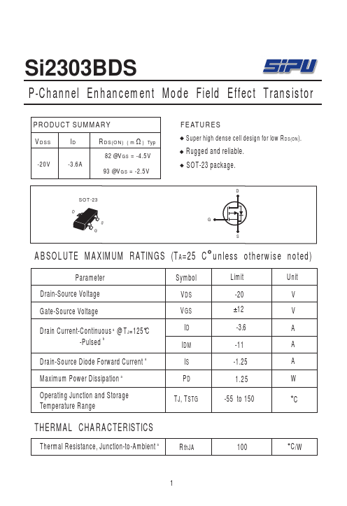
S OT-23
AB S OL UTE MAXIMUM R ATINGS (TA=25 C unles s otherwis e noted)
P arameter
S ymbol
Limit
Unit
Drain-S ource Voltage
-20
Gate-S ource Voltage
Drain C urrent-C ontinuous a @ TJ=125 C
-3.6
-P ulsed b
-11
Drain-S ource Diode Forward C urrent a
-1.25
Maximum P ower Dissipation a
Operating Junction and S torage Temperature R ange
TJ, TSTG
-55 to 150
THE R MAL CHAR ACTE R IS TICS
Thermal R esistance, Junction-to-Ambient...