SI2307BDS
SI2307BDS is P-Channel Enhancement MOSFET manufactured by Kexin Semiconductor.
Features
- VDS (V) =-30V
- RDS(ON) < 78mΩ (VGS =-10V)
- RDS(ON) < 130mΩ (VGS =-4.5V)
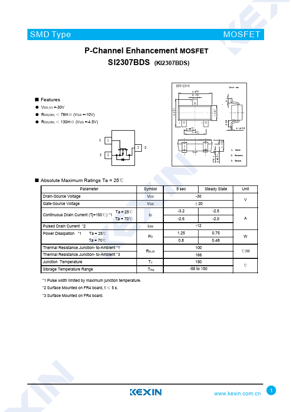
G1
S2
3D
- Absolute Maximum Ratings Ta = 25℃
Parameter Drain-Source Voltage Gate-Source Voltage
Ta = 25℃ Continuous Drain Current (Tj=150℃)
- 1
Ta = 70℃ Pulsed Drain Current
- 2 Power Dissipation
- 1 Ta = 25℃
Ta = 70℃ Thermal Resistance.Junction- to-Ambient
- 1 Thermal Resistance.Junction- to-Ambient
- 3 Junction Temperature Storage Temperature Range
Symbol VDS VGS ID IDM PD
Rth JA TJ Tstg
- 1 Pulse width limited by maximum junction temperature.
- 2 Surface Mounted on FR4 board, t ≤ 5 s.
- 3 Surface Mounted on FR4 board.
+0.2 2.8 -0.1
SOT-23-3
2.9 +0.2 -0.1
0.4 +0.1 -0.1
0.95 +0.1 -0.1 1.9 +0.1 -0.2
+0.2 1.6 -0.1
+0.2 1.1 -0.1
Unit: mm
0.15 +0.02 -0.02
1. Gate 2. Source 3. Drain
0-0.1 +0.1 0.68
-0.1
5...