SI4953ADY Overview
Key Specifications
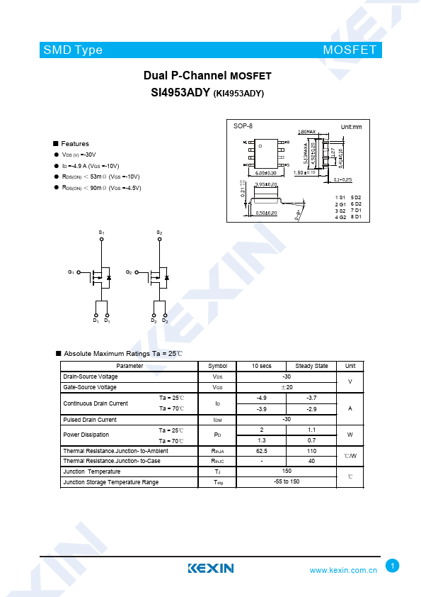
Package: SOIC
Mount Type: Surface Mount
Pins: 8
Height: 1.55 mm
Key Features
- VDS (V) =-30V
- ID =-4.9 A (VGS =-10V)
- RDS(ON) < 53mΩ (VGS =-10V)
| Part | SI4953ADY |
|---|---|
| Description | Dual P-Channel MOSFET |
| Category | MOSFET |
| Manufacturer | Kexin Semiconductor |
| Size | 1.31 MB |
Package: SOIC
Mount Type: Surface Mount
Pins: 8
Height: 1.55 mm
| Seller | Inventory | Price Breaks | Buy |
|---|---|---|---|
| RS (Formerly Allied Electronics) | 0 | 2500+ : 0.76 USD 12500+ : 0.7 USD 25000+ : 0.67 USD |
View Offer |
| Component Stockers USA | 457 | 1+ : 99.99 USD | View Offer |
| Part Number | Manufacturer | Description |
|---|---|---|
| SI4953ADY | Vishay | Dual P-Channel MOSFET |
| Si4953DY | Vishay | 30V Dual P-Channel MOSFET |
| Si4953DY | Fairchild Semiconductor | Dual P-Channel Enhancement Mode MOSFET |
| Si4953 | Nanxin | Dual P-Channel MOSFET |
| Si4953DY | TEMIC Semiconductors | Dual P-Channel MOSFET |