Si4953DY Overview
Key Specifications
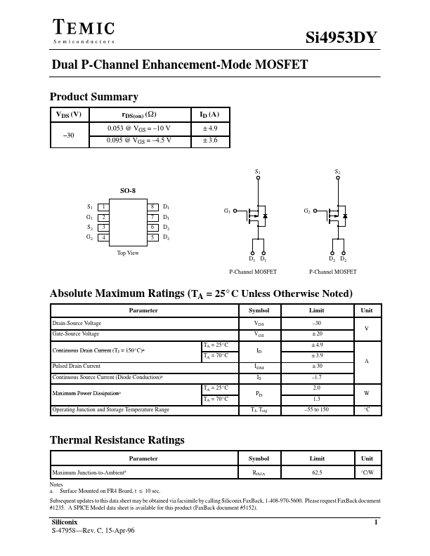
Package: SOIC N
Mount Type: Surface Mount
Pins: 8
Max Operating Temp: 150 °C
Key Features
- 10 V 0.095 @ VGS =
- 250 mA VDS = 0 V, VGS = "20 V VDS =
| Part | Si4953DY |
|---|---|
| Description | Dual P-Channel MOSFET |
| Category | MOSFET |
| Manufacturer | TEMIC Semiconductors |
| Size | 52.72 KB |
Package: SOIC N
Mount Type: Surface Mount
Pins: 8
Max Operating Temp: 150 °C
| Seller | Inventory | Price Breaks | Buy |
|---|---|---|---|
| Verical | 2500 | 373+ : 1.0073 USD 500+ : 0.9065 USD 1000+ : 0.836 USD 10000+ : 0.7454 USD |
View Offer |
| Rochester Electronics | 2500 | 100+ : 0.8058 USD 500+ : 0.7252 USD 1000+ : 0.6688 USD 10000+ : 0.5963 USD |
View Offer |
| Part Number | Manufacturer | Description |
|---|---|---|
| SI4953DY | Kexin Semiconductor | Dual P-Channel MOSFET |
| Si4953DY | Vishay | 30V Dual P-Channel MOSFET |
| Si4953DY | Fairchild Semiconductor | Dual P-Channel Enhancement Mode MOSFET |
| SI4953ADY | Kexin Semiconductor | Dual P-Channel MOSFET |
| SI4953ADY | Vishay | Dual P-Channel MOSFET |