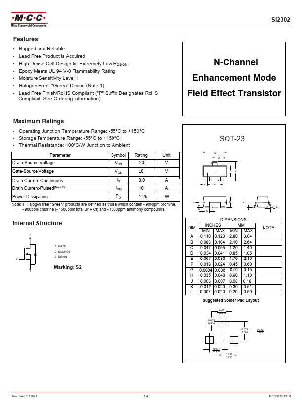
P-Channel Enhancement Mode Field Effect Transistor
Full PDF Text Transcription (Reference)
The following content is an automatically extracted verbatim text
from the original manufacturer datasheet and is provided for reference purposes only.
View original datasheet text
Features
• Rugged and Reliable • Lead Free Product is Acquired • High Dense Cell Design for Extremely Low RDS(ON) • Epoxy Meets UL 94 V-0 Flammability Rating • Moisture Sensitivity Level 1 • Halogen Free. “Green” Device (Note 1) • Lead Free Finish/RoHS Compliant ("P" Suffix Designates RoHS
Compliant. See Ordering Information)
SI2302
N-Channel Enhancement Mode Field Effect Transistor
Maximum Ratings
• Operating Junction Temperature Range: -55°C to +150°C • Storage Temperature Range: -55°C to +150°C • Thermal Resistance: 100°C/W Junction to Ambient
Parameter
Symbol Rating
Unit
Drain-Source Voltage
VDS
20
V
Gate-Source Voltage
VGS
±8
V
Drain Current-Continuous
ID
3.0
A
Drain Current-Pulsed(Note 2)
IDM
10
A
Power Dissipation
PD
1.25
W
Note: 1.