ME12P04
ME12P04 is P-Channel 40-V (D-S) MOSFET manufactured by Matsuki.
DESCRIPTION
The ME12P04 is the P-Channel logic enhancement mode power field effect transistors are produced using high cell density, DMOS trench technology. This high density process is especially tailored to minimize on-state resistance. These devices are particularly suited for low voltage application such as cellular phone and notebook puter power management and other battery powered circuits where high-side switching, and low in-line power loss are needed in a very small outline surface mount package.
FEATURES
- RDS(ON)≦45mΩ@VGS=-10V
- RDS(ON)≦80mΩ@VGS=-4.5V
- Super high density cell design for extremely low RDS(ON)
- Exceptional on-resistance and maximum DC current capability
APPLICATIONS
- Power Management in Note book
- Portable Equipment
- Battery Powered System
- DC/DC Converter
- Load Switch
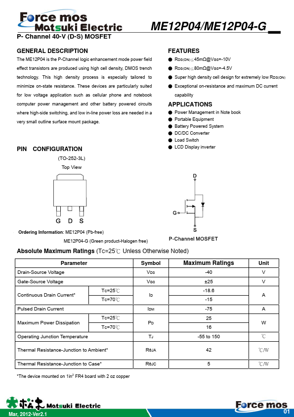
CONFIGURATION
(TO-252-3L) Top View
- LCD Display inverter e Ordering Information: ME12P04 (Pb-free)
ME12P04-G (Green product-Halogen free)
Absolute Maximum Ratings (TC=25℃ Unless Otherwise Noted)
Parameter
Drain-Source Voltage Gate-Source Voltage Continuous Drain Current- Pulsed Drain Current Maximum Power Dissipation Operating Junction Temperature Thermal Resistance-Junction to Ambient- Thermal Resistance-Junction to Case-
- The device mounted on 1in2 FR4 board with 2 oz copper
Symbol
VDS VGS TC=25℃ TC=70℃ ID IDM TC=25℃ TC=70℃ PD TJ RθJA RθJC
Maximum Ratings
-40 ±25 -18.6 -15 -75 25 16 -55 to 150 42 5
Unit
V V A A W ℃ ℃/W ℃/W
Mar, 2012-Ver2.1
ME12P04/ME12P04-G
P- Channel 40-V (D-S) MOSFET
Electrical Characteristics (TC =25℃ Unless Otherwise Specified)
Symbol Parameter
STATIC V(BR)DSS VGS(th) IGSS IDSS RDS(ON) VSD DYNAMIC Qg Qgs Qgd Rg Ciss Coss Crss Total Gate Charge Gate-Source Charge Gate-Drain Charge Gate Resistance Input capacitance Output Capacitance Reverse Transfer Capacitance Turn-On Delay Time Turn-On Rise Time Turn-Off Delay Time Turn-On Fall Time VDD=-15V, RL =15Ω ID=-1A, VGEN=-10V, RG=6Ω VDS=-20V, VGS=0V, F=1MHz VGS=0V, VDS=0V, f=1MHZ...