ML65244
ML65244 is High Speed Dual Quad Buffer/Line Drivers manufactured by Micro Linear.
DESCRIPTION
The ML65244 and ML65L244 are non-inverting dual quad buffer/line drivers. The high operating frequency (50MHz driving a 50p F load) and low propagation delay (ML65244
- 1.7ns, ML65L244
- 2ns) make them ideal for very high speed applications such as processor bus buffering and cache and main memory control. These buffers use a unique analog implementation to eliminate the delays inherent in traditional digital designs. Schottky clamps reduce under and overshoot, and special output driver circuits limit ground bounce. The ML65244 and ML65L244 conform to the pinout and functionality of the industry standard FCT244 and are intended for applications where propagation delay is critical to the system design. Note: This part was previously numbered ML6582.
FEATURES s Low propagation delay
- 1.7ns ML65244 2.0ns ML65L244 s Fast Dual 4-bit TTL level buffer/line driver with tri-state capability on the output (two 4-bit sections) s TTL patible input and output levels s Schottky diode clamps on all inputs to handle undershoot and overshoot s Onboard schottky diodes minimize noise s Reduced output swing of 0
- 4.1 volts s Ground bounce controlled outputs, typically less than 400m V s Industry standard FCT244 type pinout s Applications include high speed cache memory, main memory, processor bus buffering, and graphics cards
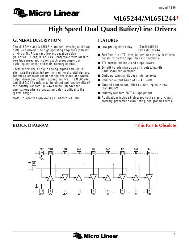
BLOCK DIAGRAM
- This Part Is Obsolete
VCC 20 VCC 2G 19 1G 1
YAO 18
BO 17
YA1 16
B1 15
YA2 14
B2 13
YA3 12
B3 11
10 GND
2 AO
3 YBO
4 A1
5 YB1
6 A2
7 YB2
8 A3
9 YB3
ML65244/ML65L244
PIN CONFIGURATION
20-Pin SOIC, QSOP
1G A0 YB0 A1 YB1 A2 YB2 A3 YB3 GND
1 2 3 4 5 6 7 8 9 10 20 19 18 17 16 15 14 13 12 11
VCC 2G YA0 B0 YA1 B1 YA2 B2 YA3 B3
TOP VIEW
PIN DESCRIPTION
NAME Ai YAi Bi YBi 1G 2G GND VCC I/O I O I O I I I I DESCRIPTION
Data Bus A Data Bus A Data Bus B Data Bus B Output Enable for data bus A Output Enable for data bus B Signal Ground + 5V supply
FUNCTION TABLE
1G/2G H L...