MT28F322D18 Overview
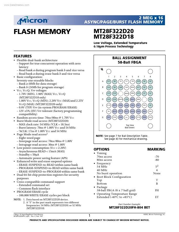
See page 43 for mechanical drawing. OPTIONS Timing 70ns access 80ns access Frequency 54 MHz 40 MHz No burst operation Boot Block Configuration Top Bottom Package 58-ball FBGA (8 x 7 ball grid) Operating Temperature Range Extended (-40ºC to +85ºC) Part Number Example: PRODUCTS AND SPECIFICATIONS DISCUSSED HEREIN ARE SUBJECT TO CHANGE BY MICRON WITHOUT NOTICE.
MT28F322D18 Key Features
- Flexible dual-bank architecture
- Support for true concurrent operation with zero latency
- Read bank a during program bank b and vice versa
- Read bank a during erase bank b and vice versa
- Basic configuration: Seventy-one erasable blocks
- Bank a (8Mb for data storage)
- Bank b (24Mb for program storage)
- VCC, VCCQ, VPP voltages
- 1.70V (MIN), 1.90V (MAX) VCC, VCCQ (MT28F322D18 only)
- 0.9V (TYP) VPP (in-system PROGRAM/ERASE)